Setting the New Standard in Electronics Design.

Efficiency. Collaboration. Accuracy.

Switch and Get the Power to Design Without Limits

Get 50% off when you switch to Altium Designer before April 26, 2024

Create Your Own PCB / Working with PCB Keepouts Completed Sign In To Save Your Progress
Click if you find this content useful

Create Your Own PCB

Working with PCB Keepouts

On the PCB, there can be specific areas that should exclude the presence of certain objects, such as vias, tracks, pads, etc. Our drone is not an exception and we need to limit the presence of copper in some areas underneath the connectors. All of this can be realized and configured in Altium Designer by using the Keepouts feature.

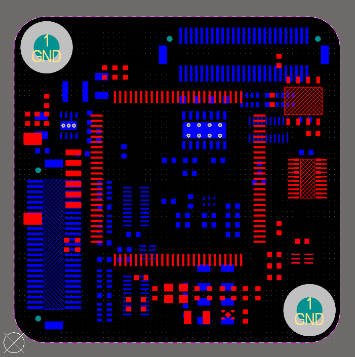
Make the Bottom layer active. Find the CN2 component. We need to create a specific area under the component to avoid copper pouring between the SMD pins rows.

CN2 component location
Fig. 1 - CN2 component location

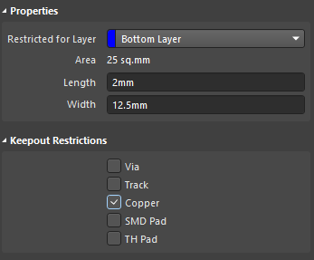
Choose Place > Keepout > Fill from the main menus. Press the Tab key to pause placement so we can configure it using the Properties panel. In the Restricted for Layer drop-down, select Bottom to make this keepout area only on the bottom layer. In the Keepout Restrictions region, select only Copper so this keepout will only restrict copper pouring in this area. Press the Tab key to resume keepout fill placement.

Keepout configuration in the Properties panel
Fig. 2 - Keepout configuration in the Properties panel
Tip: If you need to define a keepout area for all layers, select Keep-Out Layer in the Restricted for Layer drop-down menu.
 
Tip: You can place a Keepout Fill using the Active Bar.

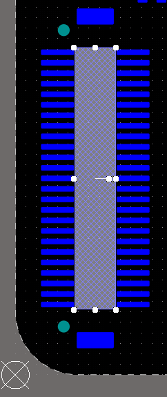
Draw a rectangle as shown in the figure below. This rectangle will restrict this PCB area from copper pouring.

Placed keepout fill underneath a CN2 component
Fig. 3 - Placed keepout fill underneath the CN2 component

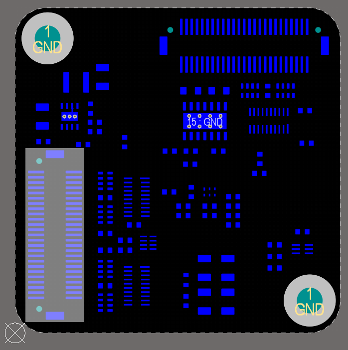
Place a keepout area with copper restriction underneath the CN3 component located on the Top Layer using the same approach. The PCB should look as shown below after placing the keepout areas.

Placed keepout areas for CN2 and CN3 connectors
Fig. 4 - Placed keepout areas for CN2 and CN3 connectors
Tip: You can use other than rectangular areas as it is done in this guide. For example, you can place a Keepout Track to which the active Clearance rule will apply for the objects selected in the Keepout Restrictions region.
Good job! Article is now completed!
Sign In To Save Your Progress

Read Again

CAPTCHA
Was this article useful?
Yes No
Thank you Glad to hear it