PCB Component Placement
Now we've come to one of the most interesting parts of the PCB design process - component placement. Competent placement of components has a huge impact on the quality of board routing and behavior. It is at this stage that a significant part of possible future problems can be solved. The correct placement of the connectors can be organized to ensure the correct ergonomics of the device. The correct placement of the power components will create good conditions for the correct function of the power-distribution network, help to avoid unnecessary voltage drop-downs, and reduce power ICs noise on high-speed ICs. Good placement of high-speed ICs allows your interfaces to run at maximum speed without any errors. Additionally, good placement of passive components will allow forming a proper decoupling and device configuration.
Correct component placement requires attention to the schematic. Some components must be placed close to each other in order for them to work correctly. Altium Designer has a Cross Probe tool that helps you to find components on the PCB by clicking on the component in the schematic and vice versa. The best way to use this tool is by working on two monitors, i.e. the PCB document and the schematic document are open on different monitors. You can use this tool by choosing Tools > Cross Probe from the main menus. Position the crosshair on any component or net then click. The software will cross probe to the item on the target document.
Let’s begin component placement.
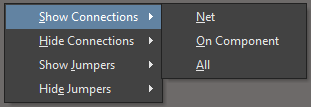
It is recommended to show all the connections between components. Open the net/connections pop-up menu by using the N hotkey. We can show/hide all the connections in general, component connections and single net connections. Select Show Connections > All to enable visibility for all connections on the PCB.
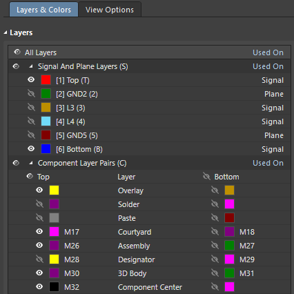
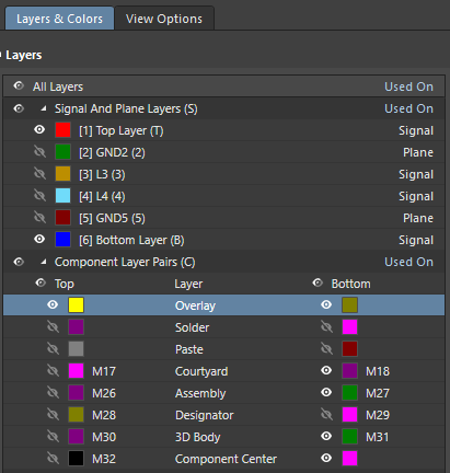
Now we will set up the view of the top layer so that there are no unnecessary or distracting layers that we do not need at this time. Open the View Configuration panel. In the Signal And Plane Layers region, make the Top and Bottom layers visible by clicking the associated eye icon for each. In the Component Layer Pairs region, make all layers under Top visible by clicking the eye icon to the left of Top and hide all layers for Bottom. Hide Solder, Paste and Designator layers for Top.
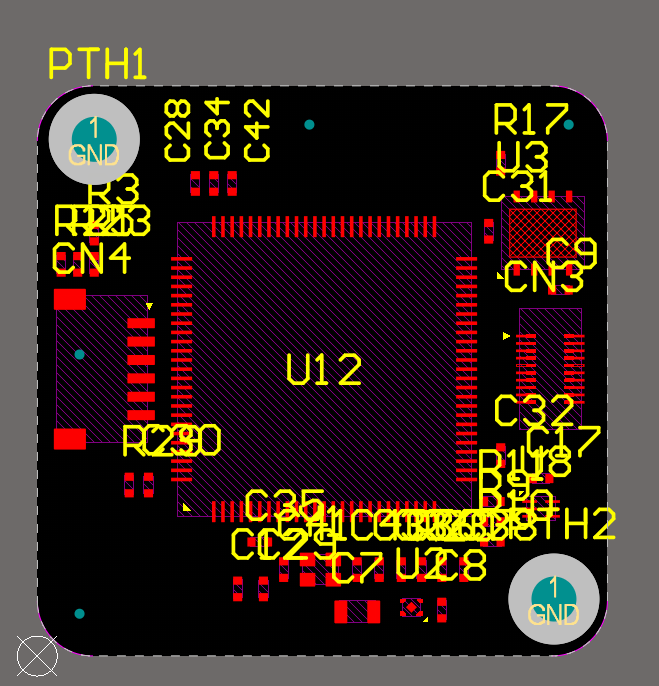
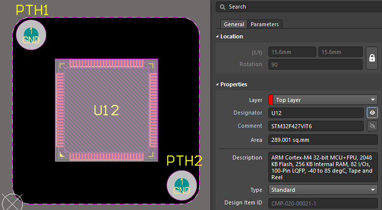
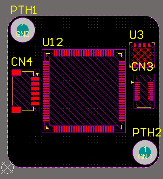
Let's place the CN3 and CN4 connectors with the U12 CPU. These are the main components on which future placement will depend. They need to be placed exactly at the X/Y coordinates. Click the U12 component to select it. Make sure that you keep the Properties panel open as it is required for parametric placement. In the Location region of the Properties panel, enter 15.6mm as the X coordinate and 15.6mm as the Y coordinate. Define the Rotation angle as 90 degrees. At this rotation angle, future routing will be optimal in terms of PCB design. Now our CPU is located exactly at the PCB center and we need to lock its movement to avoid possible errors. This is done by clicking the Lock icon.
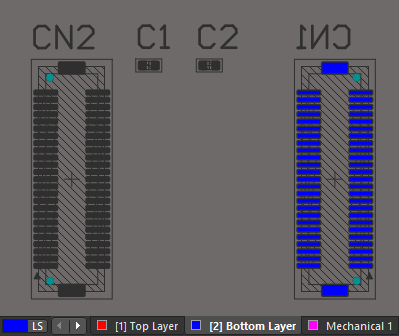
Place the following components at the listed locations on the Top Layer and lock them:
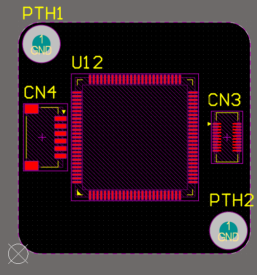
- CN3 - (X/Y) (27.9mm/15.6mm), Rotation 270
- CN4 - (X/Y) (3.2mm/15.6mm), Rotation 270
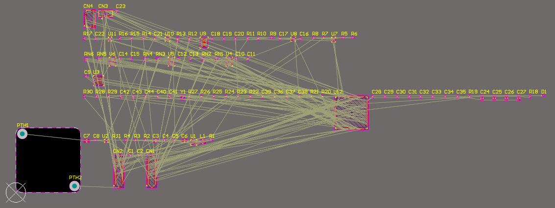
Your PCB should now look as shown below.
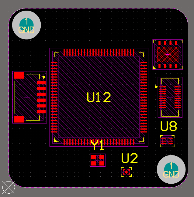
Hover your mouse over the U3 component then click and hold to select it. Drag the component while holding down the mouse button. While moving the component, you can rotate it counterclockwise 90 degrees by pressing the Spacebar. Rotate the U3 component 90 degrees then place it above the CN3 connector and to the right of U12 as shown below.
Place the U2, U8, and Y1 components as shown below
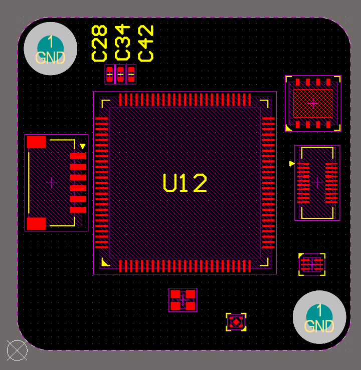
Find components C28, C34 and C42, and place them above U12 in accordance with net lines. You can align components to make the placement tidy. Select all placed components, right-click then select Align > Align Top or Align Bottom from the context menu. You also can evenly distribute the selected components by right-clicking on any of the selected components then choosing Align > Distribute Horizontally.
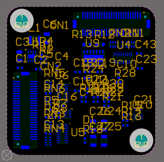
Up to now, we placed components on the top side of the PCB. Now let’s place several components on the bottom side. There are two ways to set the layer of placement: in the Properties panel while the component is selected, and by using the L hotkey while the component is being moved/dragged.
Before component placement on the bottom layer, it is recommended to set up layer visibility as we did for the top layer placement. Open the View Configuration panel. In the Component Layer Pairs region, show all layers for Bottom and hide all layers for Top except Top Overlay. Hide the Solder, Paste and Designator layers for Bottom.
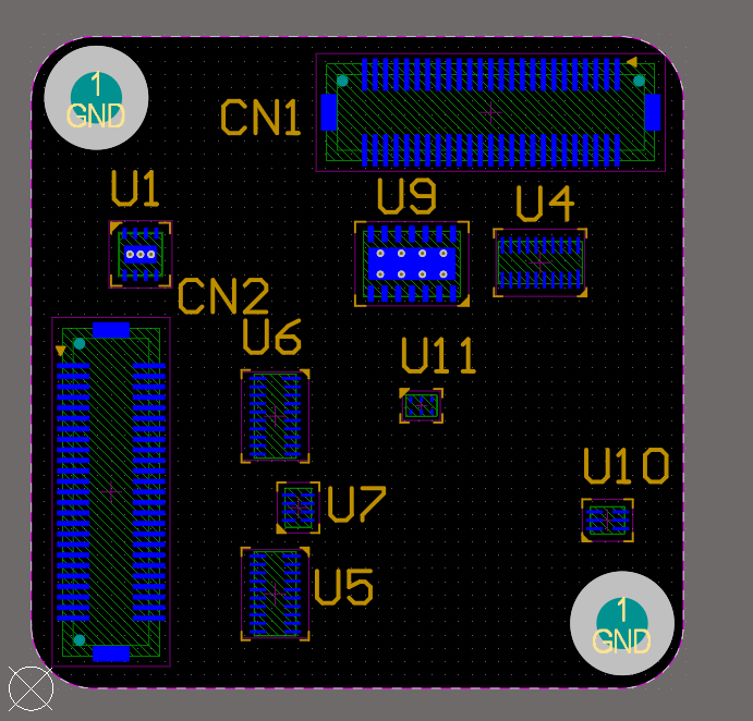
Select the CN1 component. Use the Layer drop-down in the Properties panel to set it to Bottom. The component is now located on the bottom layer. Place it at coordinates X: 21.85mm and Y: 27.4mm and the Rotation at 180 degrees then lock it. Now continue placing the following components on the bottom layer at the following coordinates and rotations, then lock them.
CN2 : X/Y at 3.8mm/9.35mm, Rotation 270 degrees
U1 : X/Y at 5.2mm/20.65mm, Rotation 270 degrees
U4 : X/Y at 24.2mm/20.25mm, Rotation 90 degrees
U5 : X/Y at 11.6mm/4.5mm, Rotation 180 degrees
U6 : X/Y at 11.6mm/12.95mm, Rotation 180 degrees
U7 : X/Y at 12.7mm/8.6mm, Rotation 180 degrees
U9 : X/Y at 18.1mm/20.2mm, Rotation 90 degrees
U10 : X/Y at 27.4mm/8mm, Rotation 360 degrees
U11 : X/Y at 18.55mm/13.45mm, Rotation 270 degrees
Now you have learned all the basic component placement skills you will need and also how to manage the visibility of the layers so there’s nothing stopping you from completing the full PCB component arrangement. Show your imagination! If you're stuck, you can look at the images below to make sure you are placing the components correctly. You can flip your PCB by using the Ctrl+F key combination for more comfortable component placement on the bottom PCB side.