

Resolving Schematic Errors
Now that you have validated your project, we sincerely hope that there are no errors in it. However, if errors are present in your project, this chapter will explain how to correct them and avoid their appearance in the future.
Violations Associated with Components
Component revision is Out of Date
Reported in the Messages panel as a Warning █.
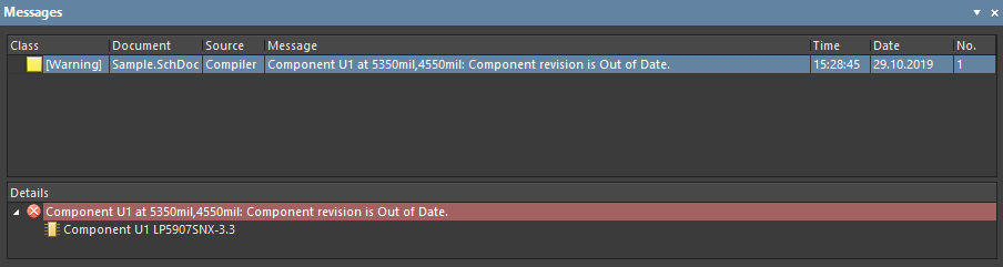
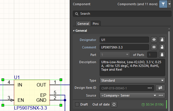
This error is due to the use of an outdated component in your project. It usually happens when the schematic was developed some time ago and the components on the server have been changed and a new revision was created during the schematic development cycle. It is extremely important to use the most current components in the design since they are free from errors that were in previous revisions. To view the component causing the violation, double-click on the details. Notice that the current state of this component is defined as Out of date in the Properties panel.
Depending on the number of outdated components, there are two approaches to correcting this error.
- If your project has a few outdated components, it is better to update them manually. Select the desired component then click on the update icon to the right of the component status in the Properties panel. Clicking on the icon will start the update process and when it is finished, the new status of the component will be displayed.
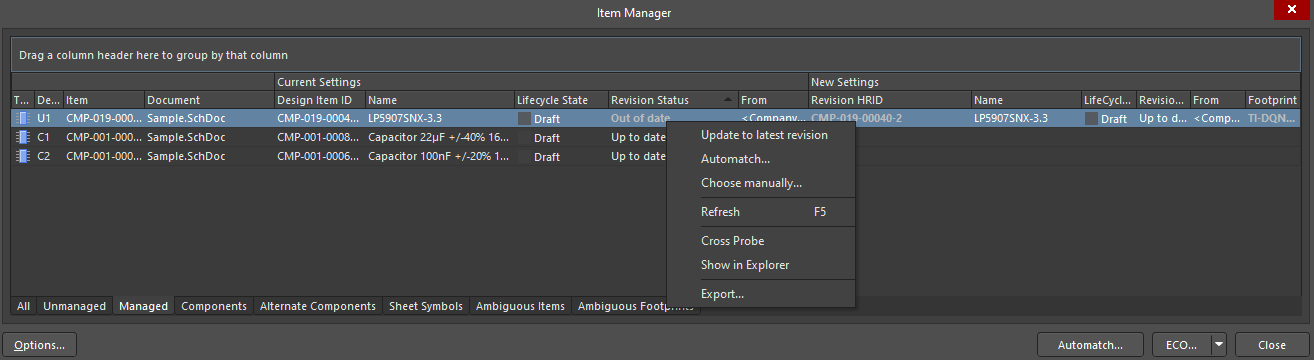
- If your project has many outdated components, it will be easier to update them using the Item Manager dialog, which is accessed by choosing Tools > Item Manager from the main menus. In the Item Manager dialog, all components used in your project are displayed in a table. Select the Managed tab in the lower-left corner to show only managed components used in your design. Click on the Revision Status column name to sort by the value and to show outdated components at the top of the table. While holding Ctrl or Shift, select all components that have an Out of date status. Right-click on any selected component then choose Update to latest revision from the context menu. After updating, the updated component parameters are displayed on the right side of the table. Click the ECO button in the lower right corner of the dialog then select Generate ECO to apply the changes. In the Engineering Change Order dialog that opens, click Execute Changes.
If you now see Up to date as the component status in the Properties panel, you did everything right. The component is current and there are no more violations.
Duplicate Part Designators
Reported in the Messages panel as an Error █.
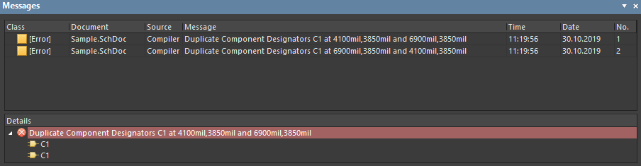
This error usually occurs if the component designators have been assigned manually without using the Annotate Schematics command. If you select an error in the Messages panel, you will see a list of components with the same designator in the Details region. Double-click on a component in the Details region to view that component in the schematic.
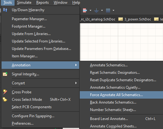
As a rule, if you have made a mistake with designators, manual correction of the Designator value in the Properties panel may not help. To fix this error, you need to perform forced annotation. Choose Tools > Annotation > Force Annotate All Schematics from the main menus. In this process, Altium Designer will automatically check all designators and reannotate them if there is a deviation in the component numbering logic.
When the work is finished, a dialog opens that shows the number of updateable designators. Select Yes to proceed with the changes.
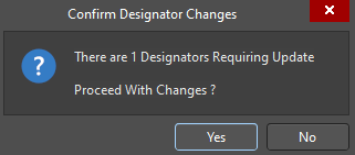
After confirmation, all incorrect designators will be corrected automatically. Updated designators will have the previous designator in parentheses, which will disappear after project compilation.
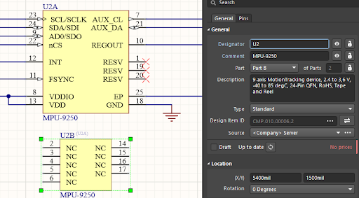
Unused Sub-part in Component
Reported in the Messages panel as a Warning █.
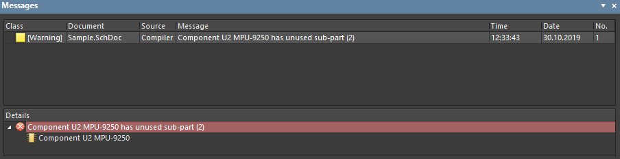
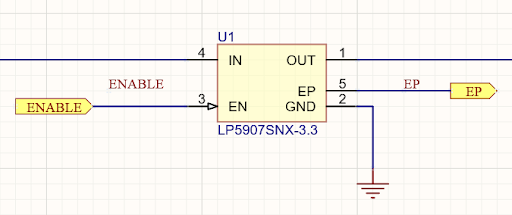
This is one of the mistakes you wouldn't notice at first glance. It occurs when you have components in the project that are separated into functional parts and one of the parts is not placed in the schematic. You can see such symbols by the Designator mask X?A, where A is an ordinal symbol of a multipart component.
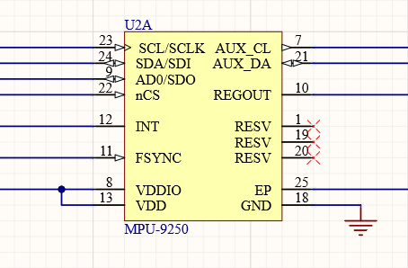
Fixing this error is easy. The error text in the Messages panel shows that part of the component that was not placed. In the example shown in Figure 10, this is sub-part (2). Double-click on the component in the Details region to zoom to the component. Copy the selected component then place it on any free (blank) place on the schematic. Select the copied component then open the Properties panel so you can define this component as required. Unlock the Part field by clicking on the lock icon to the right of the field (if it is locked). In the drop-down menu of the Part field, select the required part. In this case, we need to place Part B. The part symbol will be automatically updated after sub-part selection. You also need to specify the same Designator as the previously copied component.
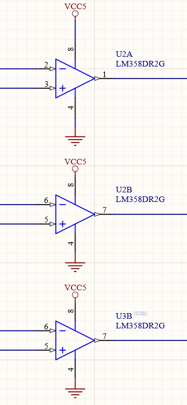
Components containing duplicate sub-parts
Reported in the Messages panel as an Error █.
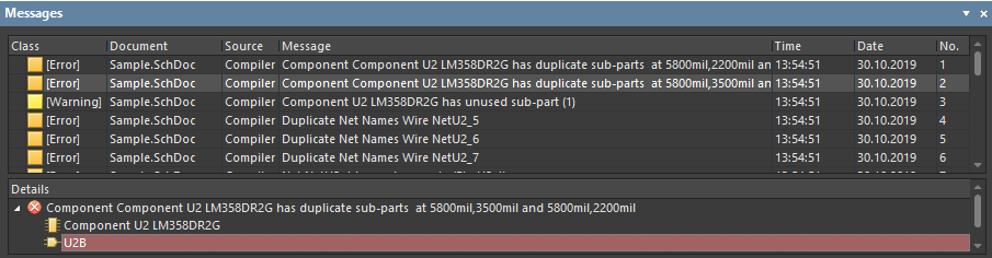
This error happens when one sub-part of a multipart component has been placed more than once in a schematic. This violation causes several other related errors such as Unused sub-part (for an abnormal copy of component sub-parts) and Duplicate Net Names Wire (same net naming for pins).
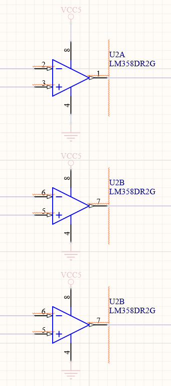
If the placement of the second sub-part of the component was done by mistake, delete the unnecessary sub-part of the component to fix the error. However, if you need to use this component part in your design, you need to increment its Designator to avoid breaking the rules. Use the forced annotation process by choosing Tools > Annotation > Force Annotate All Schematics from the main menus. During the process, Altium Designer will automatically check all designators and reannotate them if there is a deviation in the component numbering logic. After the process, the error will be gone and you will be able to use the component as usual, but you will need to buy and place one more component in your PCB.
Violations Associated with Nets
Floating Net Labels/Floating Power Objects
Reported in the Messages panel as a Warning █.
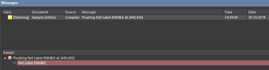
This violation appears if a schematic sheet presents a NetLabel/Power Port object that is not attached to any wire.
Always pay attention to the bounding crosshairs when placing any objects on the schematic sheet - Net Labels and Power Ports are no exception!
To fix this violation, you need to locate the violating Net Label or Power Port by double-clicking on it in the Details region. Connect the floating object to the desired wire while paying attention to the bounding crosshair. If you're sure you do not need this object, remove it from your project.
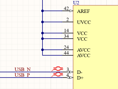
Missing Positive/Negative Net in Differential Pair
Reported in the Messages panel as an Error █.
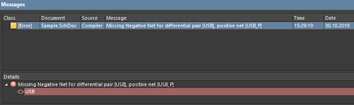
This error happens when there is no positive/negative net in a particular differential pair, while the opposite net does exist. The principle of differential signal transmission is based on the use of two wires with anti-phase signals transmission to protect the signal from external interference. In order for these wires to be processed correctly by Altium Designer, a few rules must be observed:
- For both differential pair wires, the Differential Pair directive must be placed.
- The net name must contain the suffix _N for negative net and _P for positive net.
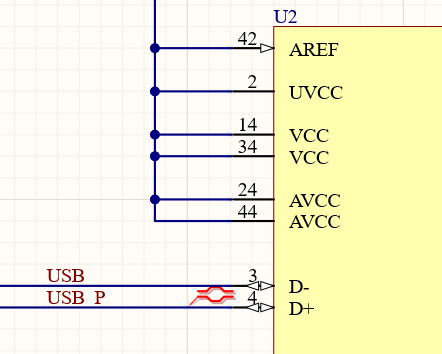
To correct this violation, locate the violating differential pair wire and make sure that the Net Label and the Differential Pair directive are attached to the net and that the net name is defined correctly.
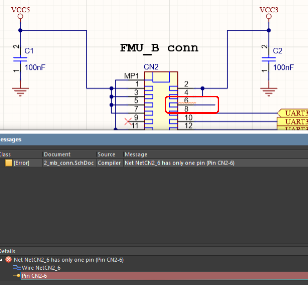
Nets with only one pin
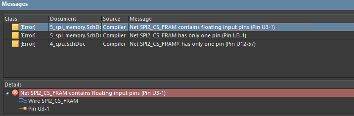
Reported in the Messages panel as an Error █.
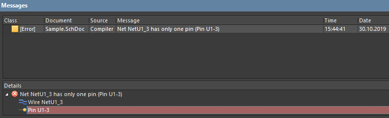
This error occurs if one of the net pins is not connected to any other object on the entire schematic design. This error can also be caused when the net with the port is placed on one sheet and has no corresponding port on other sheets. In that case, a separate warning of “Net contains floating input pins” will be shown in the Messages panel.
This error can be fixed using one of the following approaches:
- If the violating net needs to be connected, connect it to the corresponding schematic object (port, power port, net, another pin) to create a connection.
- If this net should not be connected as part of the schematic design, place a No ERC directive on it to exclude this net from the design rule check. You will learn more about the No ERC directive below.
Violations Associated with Documents
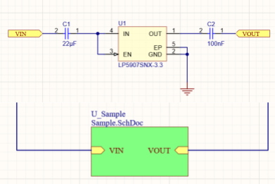
Sheet Entry not matched
Reported in the Messages panel as an Error █.
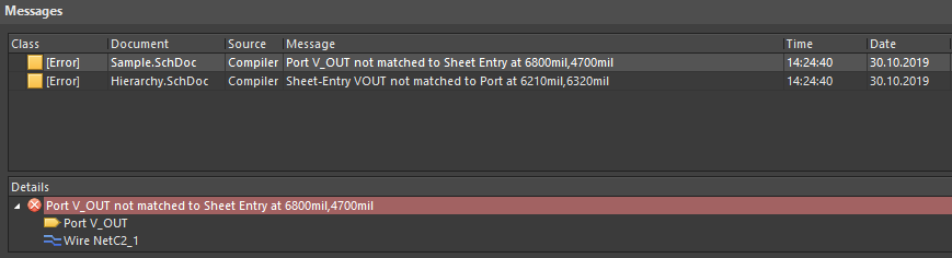
This violation occurs when there is no matching between the child sheet ports and the parent sheet entries. In general, such an error occurs if one of the Sheet Ports has been renamed after Sheet Symbol generation, or if the Sheet Entry on the Sheet Symbol was incorrectly specified manually without using auto-generation.
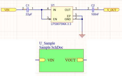
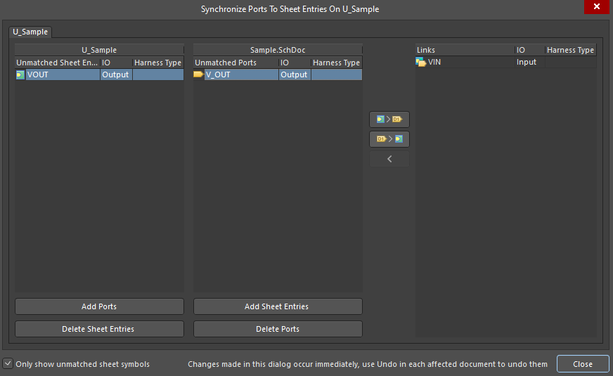
The Details region of the Messages panel shows the specific Sheet Port/Sheet Symbol that is causing the violation. You can correct their names manually, or you can start the Sheet Ports to Sheet Entries synchronization by right-clicking on the Sheet Symbol then selecting Sheet Symbol Actions > Synchronize Sheet Entries and Ports. In the Synchronize Ports to Sheet Entries dialog that opens, select the Sheet Entry on the left side of the dialog and the Sheet Port in the middle section then click the button with the desired type of synchronization.
-
The
 button will change the Sheet Port name based on the Sheet Entry name.
 -
The
 button will change the Sheet Entry name based on the Sheet Port name.
After pressing the desired button, all ports will be converted to a single form and the violation will be fixed.
No ERC Directive
The No ERC (No Electrical Rules Check) directive is a special schematic object used to disable all or some of the rules on a particular schematic object. If a particular schematic object causes a compilation error and you are sure that it is not a mistake or this violation will not affect the device's performance in any way, you need to place this directive. A No ERC directive supports a number of different styles and can be set to any color. Use this feature to reflect your design intent at this point in the design.
You can place it in the following ways:
- Right-click on any object then select Place > Directives > Generic No ERC.
- Select Generic No ERC from the Active Bar.
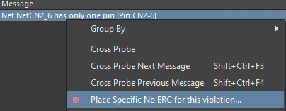
- Right-click on a violation in the Messages panel then choose Place Specific No ERC for this violation.
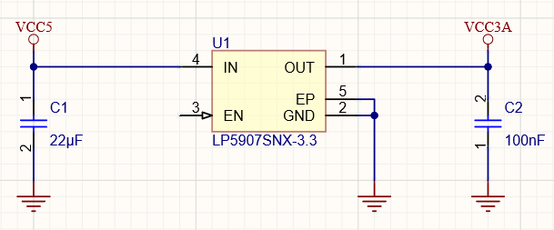
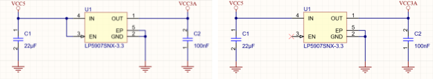
We have a violation with a floating input component pin and we know that this component pin should not be connected to any schematic net.
The process of No ERC directive placement does not differ from the usual schematic placement. The directive should be placed exactly at the violating component pin. Let's use directive placement from the Messages panel. Right-click on the violation in the list then select Place Specific No ERC for this violation.
Altium Designer will zoom to the violating component pin and automatically attach a crosshair to the cursor with a directive symbol. Place the No ERC directive at the edge of the pin line. In the Properties panel, the No ERC parameters, color, symbol, and suppressed violations are displayed.
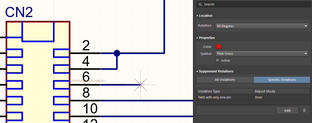
We can add a set of specific suppressed rules or completely suppress all the rules for this directive. To suppress all violations, select the directive in the design space then select All Violations in the Properties panel. For Specific Violations, select the directive in the workspace then choose Specific Violations in the Properties panel. Click the Add button to open the No ERC dialog.
Tip: If you place a No ERC directive using the Active Bar or Place menu, it will automatically suppress all violations.
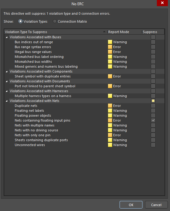
In the dialog, with Violation Types selected at the top, you can select/deselect rules that will be suppressed with the selected No ERC directive. You can also customize the connection matrix for the selected directive by selecting Connection Matrix at the top of the dialog. In this region, you can select connections that will be suppressed by this directive.
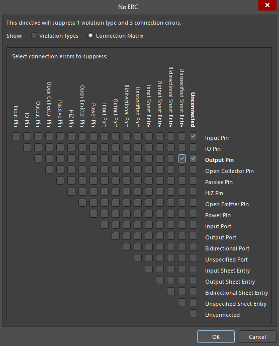
After specifying the necessary suppressions, close the No ERC dialog. Now the project will not generate an error for the objects that are connected to this directive.