Polygon Pouring for Good PDN
The next step is to properly create a power supply system. Each track has its own current limit that it can pass through without being destroyed. This value depends on the width, thickness, and horizontal and vertical distance to the reference plane layer. In common signals, currents are minimal, but in power nets, currents can reach several amperes. For this reason, polygons are mainly used for the quality and reliability of the power supply system. The IPC-2152 standard is used to calculate the minimum conductor width.
Earlier in the routing stage, we formed a power distribution network by using ordinary tracks of increased width. This approach is acceptable, but in order to increase reliability, it is recommended to present power nets as polygons. It is very convenient to work with visually separated nets, so let's define colors for the VCC5 and VCC3 nets.
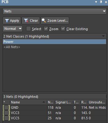
Open the PCB panel then select Nets from the top drop-down menu. Earlier, we created a Power Net Class. Activate it by clicking on the net class name.
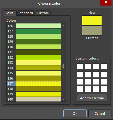
Right-click on VCC3 in the net list then select Change Net Color and select any color from the list. Press OK to save the color for the net.
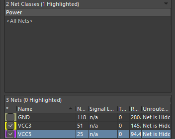
Change the color for the VCC5 net using the same approach. The net list should now look like the figure below. Turn on the color display override by checking the box next to each net. If the color of the nets on the PCB have not changed after this step, press F5 to turn on color overlay.
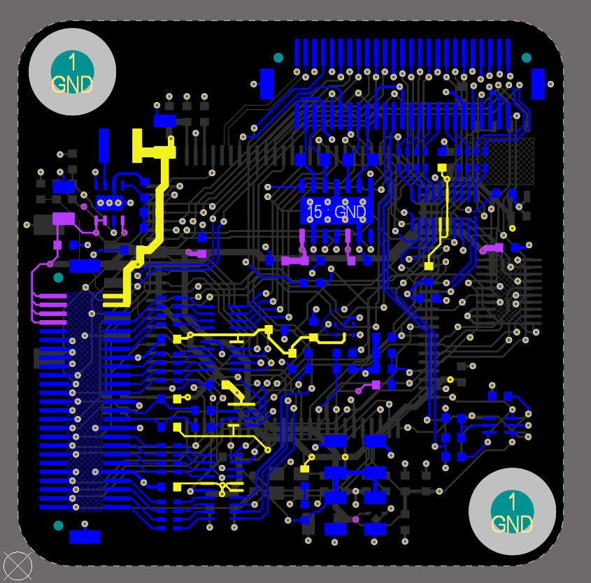
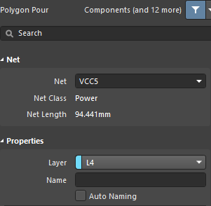
Make Layer [4]L4 the active layer. Let’s create a polygon connection for a VCC5 net located on this layer. Choose Place > Polygon Pour from the main menus. When the crosshair appears in the design space, press Tab to pause placement and edit the parameters of the polygon in the Properties panel. In the Net field, use the drop-down to select VCC5. Press the Tab key to continue polygon placement.
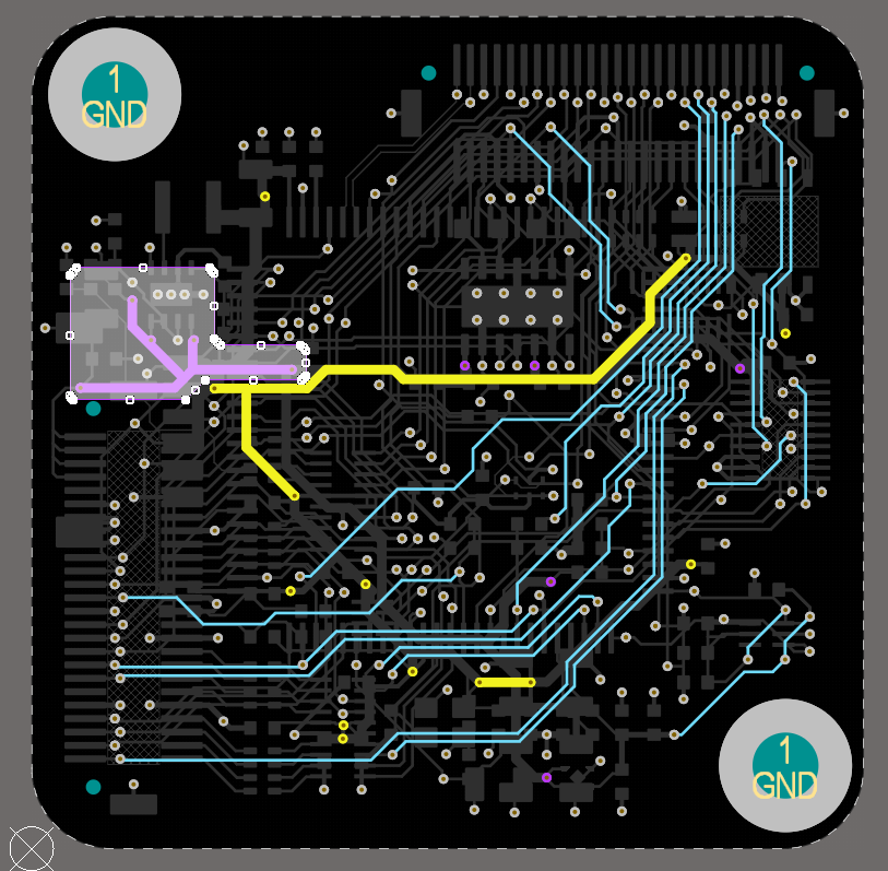
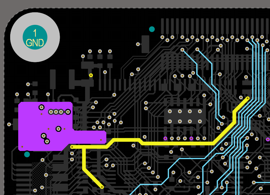
Make sure that the drawing mode is Line 45/90 in the status bar. If another drawing mode is activated, switch it by pressing Shift+Spacebar until the Line 45/90 mode becomes active. Draw a polygon by clicking along the contour of the placed tracks of the VCC5 net as shown in the figure below. You can switch the drawing angle by pressing the Spacebar. Right-click to exit polygon placement.
Right-click on the polygon. Select Polygon Actions > Repour Selected to fill this shape with copper. After pouring, the polygon will be connected to the previously placed track using thermal relief, which we do not need. There are two ways to solve this situation. The first is just to remove the placed track since we do not need it anymore. After it is removed, repour the polygon again. The second is to configure the polygon pouring options in the Properties panel by selecting the polygon and using the drop-down in the Properties region to set it to Pour Over All Same Net Objects. After changing the pouring mode, repour the polygon. The final polygon should look like the figure below.
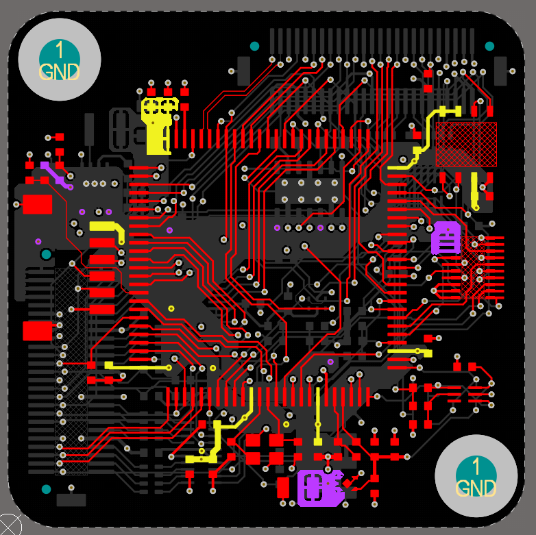
Using this approach for polygon creation, create polygons for nets VCC3 and VCC5 on all layers where those nets are present.
You can modify the polygon border of a polygon at any time by moving the handles that appear when a polygon is selected. Always remember that the wider the polygon, the more current it will hold and the more reliable the printed circuit board will be. You can calculate the current threshold for a given polygon width using the IPC-2152 standard. For example, there is a conductor with a width of 0.2 mm located in the inner layer of the PCB with a thickness of 1.5mm and a distance of 0.15mm to the reference plane. This conductor is able to withstand a current of ~0.88 amperes. Conductors with a width of 0.3mm in the same configuration can withstand 1.2 amperes and a 0.5mm conductor can withstand 1.8 amperes. It is also recommended to place faces of polygons at an angle of 45 degrees to each other. Sharp corners may increase current density that can lead to overheating of the PCB and possible copper burnout. However, on the outer layers, the copper thickness is higher due to the finish coating, so the conductors on the outer layers are able to withstand much higher current. For example, a conductor with 0.5mm width, made of 18um copper foil and plated with 35um finish coating with a board thickness of 1.5mm and the distance to the reference range 0.15mm can withstand 3 amperes without any problems. Your PCB with placed polygons for nets VCC3 and VCC5 nets should look like the figure below.
![Polygon placement for Layer [3]L3](http://files.my.altium.com/sites/default/files/inline-images/image15_1.png)
![Polygon placement for Layer [4]L4](http://files.my.altium.com/sites/default/files/inline-images/image5_10.png)
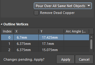
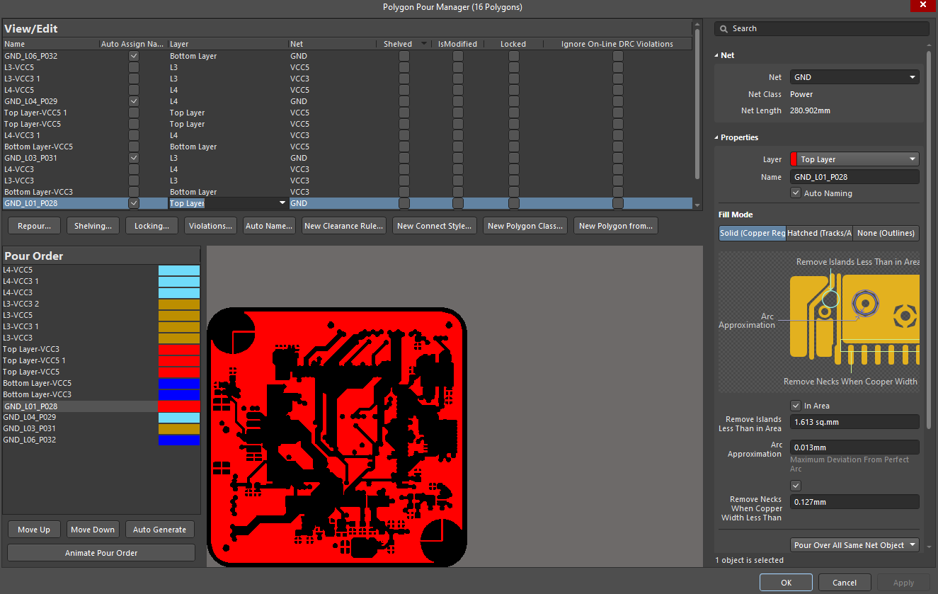
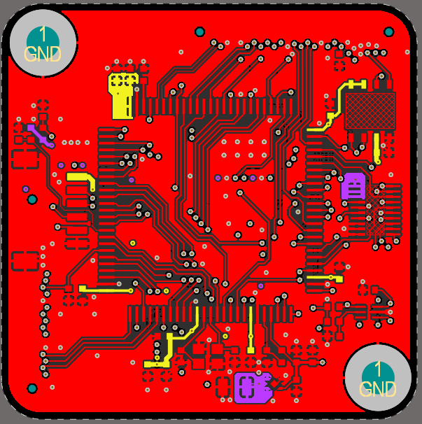
We need to fill the empty space with a grounding polygon to ensure copper balance. It can be done quickly using the Polygon Pour Manager dialog, which is accessed by selecting Tools > Polygon Pours > Polygon Manager from the main menus. The top region of the dialog contains a list of all polygons that are placed on the PCB. Click the New Polygon from button then select Board Outline from the menu as a source for the new polygon. A new polygon will appear in the list that is not connected to any net, so we need to define a GND net for it. Select the polygon in the list then on the right side of the dialog in the Properties region, use the Net drop-down to select GND, use the Layer drop-down to select Top. In the drop-down below the image, use the drop-down to select Pour Over All Same Net Objects as the pouring mode. Click Apply at the lower right corner of the Polygon Pour Manager dialog to confirm the changes.
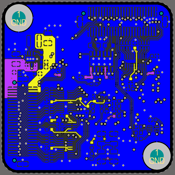
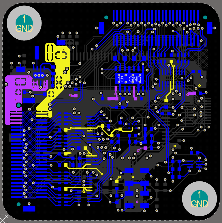
Create GND polygons from the board outline for layers [3]L3, [4]L4 and the Bottom Layer using the same approach. Close the dialog once completed. The final result should look like the figure below
![Finished polygon creation for Layer [3]L3](http://files.my.altium.com/sites/default/files/inline-images/image6_7.png)
![Finished polygon creation for Layer [4]L4](http://files.my.altium.com/sites/default/files/inline-images/image3_15.png)