

Routing Post Processes
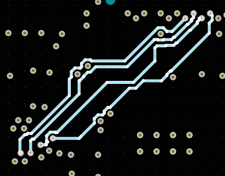
Once the PCB routing is complete, you should take a final look at the result of your work before starting the Design Rule Check. At this stage, you could find track placement defects, and also optimize the topology because focused attention while routing usually concentrates on the individual functional parts of the board and not all of the PCB as a whole. To optimize the already placed topology, Altium has a separate tool called Gloss.
Gloss Tool
The Gloss tool is used to optimize tracks by reducing the length and the number of unnecessary corners. This tool thoroughly analyzes selected tracks and automatically makes them more accurate. This tool can be used as outlined in the following steps.
Select a track or group of tracks whose routing needs to be improved.
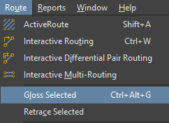
Select Route > Gloss Selected from the main menus to apply the Gloss tool to selected tracks.
Depending on the number and complexity of the selected tracks, the application of this tool may take some time. As a result, the routing of the selected tracks will be automatically improved.

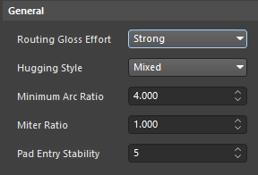
In some cases, the Gloss tool may not be configured by default. You can adjust the processing intensity on the PCB Editor - Interactive Routing page of the Preferences dialog in the General region by selecting the desired intensity in the Routing Gloss Effort drop-down menu.
Retrace Tool
The next tool that can save a lot of time while correcting topology is the Retrace tool. During PCB design, there can be cases when it is necessary to change the rules for routing. For example, you may need to increase the width for the power net or to change parameters, such as the width of the track and the gap between them in a differential pair. (This would need to be done when the printed circuit board material has changed and the tracks need to be reconfigured to match the value of the target impedance.) Once the rules are updated, all placed tracks are not automatically updated.
You now have a decision to make. You can either route the tracks manually and spend precious time on it, or you can use the Retrace tool. While Gloss tries to reduce the total length of traces and the number of angles, the Retrace tool applies the preferred values of width and gaps from the rules to existing traces. With the Retrace tool, you can easily reduce or increase the width of a selected set of chains and even the width and gaps of differential pairs. Below is an example of how this tool works.
Let's imagine that the selected manufacturer cannot produce the designed PCB due to the lack of the specified material. So, if there are tracks with controllable impedance in the project, they must be updated to meet the new requirements. Previously, a separate rule was created where the trace of the differential pair on the top layer was performed based on the specified impedance profile, which depends on the printed circuit board material. Let’s change the material and update the differential pair to meet new rules by using the Retrace tool.
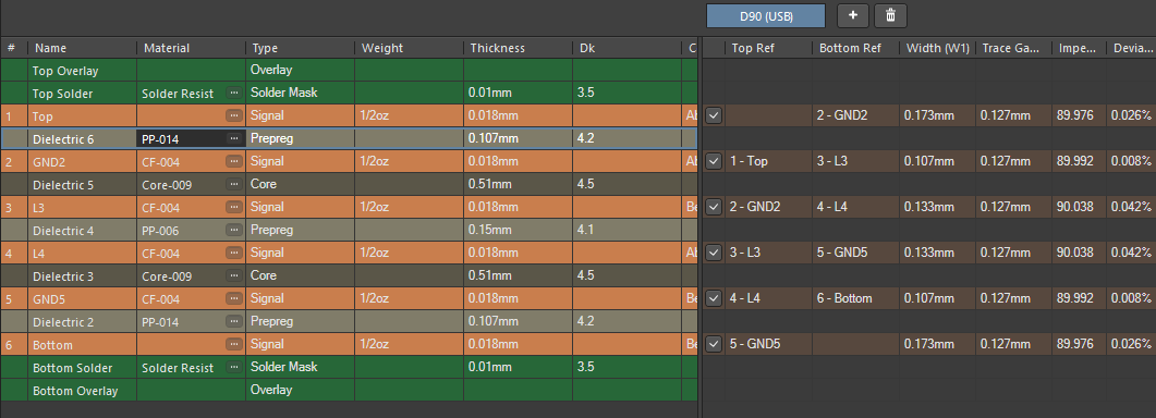
Select Design > Layer Stack Manager from the main menus. Select the Impedance tab at the bottom of the workspace. We will address the Width and Gap values for the differential pair.
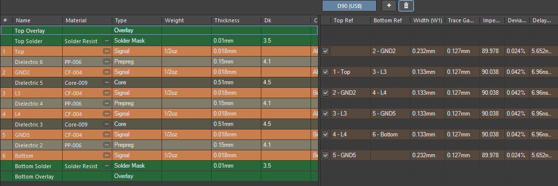
Change the Material of Dielectric 6 from PP-006 to PP-014 by clicking the ellipsis on the right side of the cell then selecting PP-014 from the Select Material dialog. All impedance profiles will be automatically updated. Save the Stackup document by right-clicking on the document in the Projects panel then choosing Save to PCB then open the PCB document.
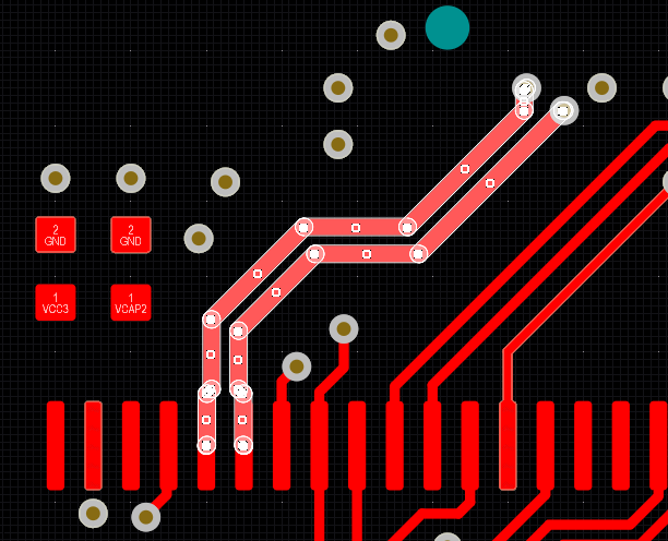
On the top layer, select the USB differential pair.
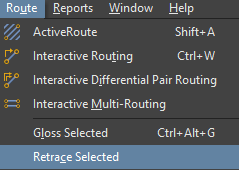
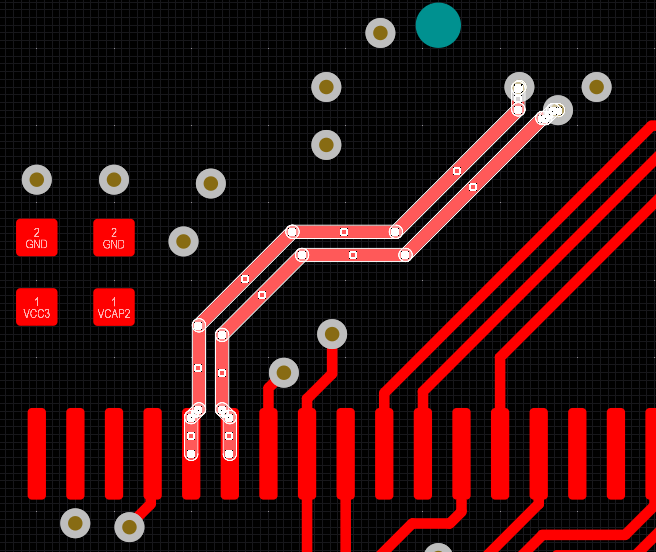
Select Route > Retrace Selected from the main menus. After applying this tool, the width and gap values of the differential pair will be updated automatically.
This tool also allows you to work with any rule changes not bound to a set of layers. For example, you can change the Preferred Width value for the Power Net class and apply the Retrace tool to the corresponding tracks.