Using Net Labels
Altium Designer allows two types of connections between components: physical and logical. The physical connection is represented as a wire between the component pins since they are physically connected to each other.
However, it is also possible to have a logical connection created by placing the names of the circuits on the placed wires. In this way, the components can be placed at any distance from each other within the sheet.
In addition to providing a logical connection, the Net Label allows you to specify names for nets. Labeling of the circuit name provides a simpler and more humanly-understandable interaction (e.g., compare the names "NetJ4_3" and "D+". Which one is more clear and understandable?). It is also much easier to create rules and customize the appearance of the marked traces during PCB routing, which you will see in future chapters. First, let's specify names for the two nets placed on the current sheet using a net label. To label the net, start the Net Label placement tool ( ) located in the Active Bar or Place > Net Label in the main menus. Let’s label several nets.
Run the Net Label tool. A crosshair with a text label will be attached to the cursor.
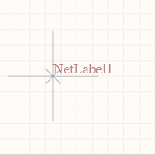
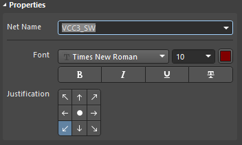
Press Tab to pause net label placement. In the Name field in the Properties panel, enter VCC3_SW (this will be a future net name). Press Tab again to return to placement mode.
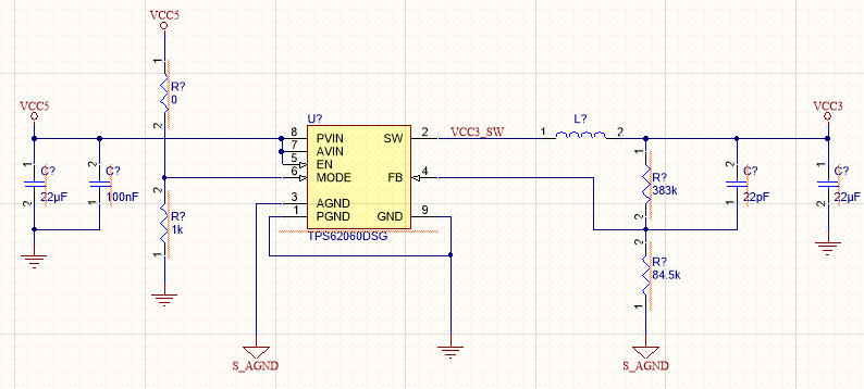
Place the configured net label on the net as shown at the figure below.
Warning: The blue crosshair should appear before placement!
Tip: You can place a net label on any type of wire or wire grouping, such as a Bus or Harness.
Place the VCC3_FB net label on the wire at pin 4 of the current component.
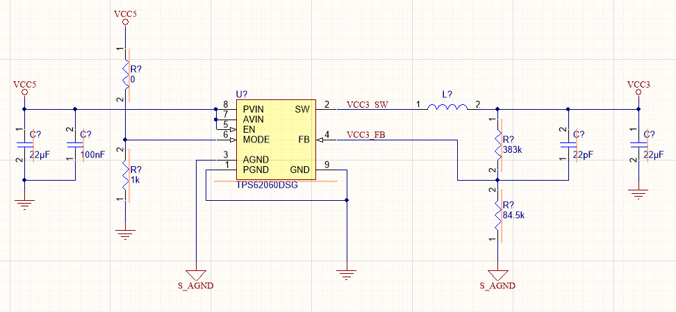
Nice work! No other net labels are required on this schematic sheet.
Now let's create a logical connection on one of the schematic sheets. The Kame_FMU project contains the document 4_cpu.SchDoc. Double-click on the file name in the Projects panel to open it.
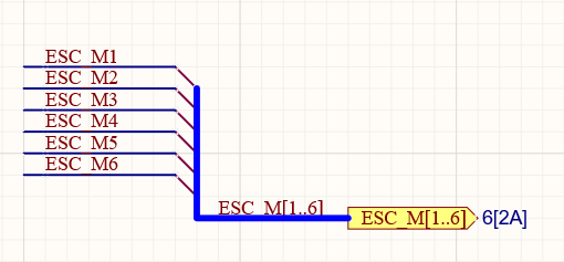
On the lower-left of the schematic sheet, there is a bus with signals of the ESC_M group with a connected port. On each wire from the bus, you need to place a net label to provide a logical connection to the same-named nets that are already placed on this sheet.
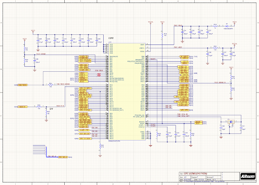
Run the Net Label tool. Define the name ESC_M1 in the Properties panel then place the Net Label on the top wire of the bus group. Note that after placing the first net label, the name for the next one has been automatically changed to ESC_M2, which allows you to place ordinal names without needing to name them manually.
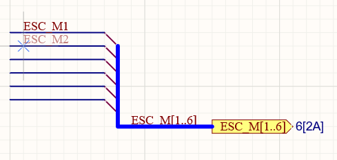
Place the net labels for the remaining wires in the bus group as shown below. The logical connection between the bus group and the MCU pins is now established. Save the 4_cpu.SchDoc sheet then return to the 3_power.SchDoc sheet.