Configuring the Basic Rules
Correct rules definition is a very important step in the PCB design process. These rules describe to CAD the restrictions for manufacturing, impedance control, and routing parameters, and what can and cannot be done within the design. These rules cover everything from the minimum width of the conductor to the maximum height of the component in a particular area of the PCB. Any mistake or failure to comply with the rules can lead to problems, up to and including the complete inoperability of the PCB or the impossibility to manufacture or assemble it. Rules in Altium Designer are presented in the form of a hierarchy - from the fundamental rules covering the entire board to the rules of individual net classes. The rules in Altium Designer are set up using the PCB Rules and Constraints Editor dialog, which is a modern and powerful tool for design rules management.
You can access the PCB Rules and Constraints Editor dialog at any time your PCB is open by selecting Design > Rules from the main menus. You will soon see that setting even the most complicated rules in Altium Designer is incredibly easy and clear. Let’s set the design rules for our drone PCB.
First, we need to configure a basic rule for net-to-net clearance for all nets in our PCB.
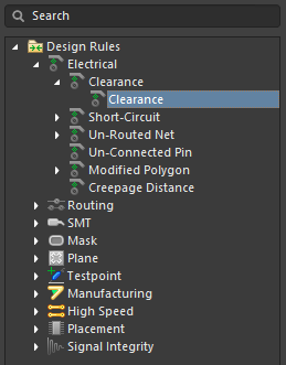
Open the PCB Rules and Constraints Editor dialog. In the left pane of the dialog, there is a list of the types of rules you can set. Expand the Electrical region then expand the Clearance sub-region. There is a single Clearance rule, which we will configure.
Select Clearance. On the right side of the dialog, the current rule settings are displayed. Under the Constraints region, set the Minimum Clearance to 0.1mm for Different Nets Only.
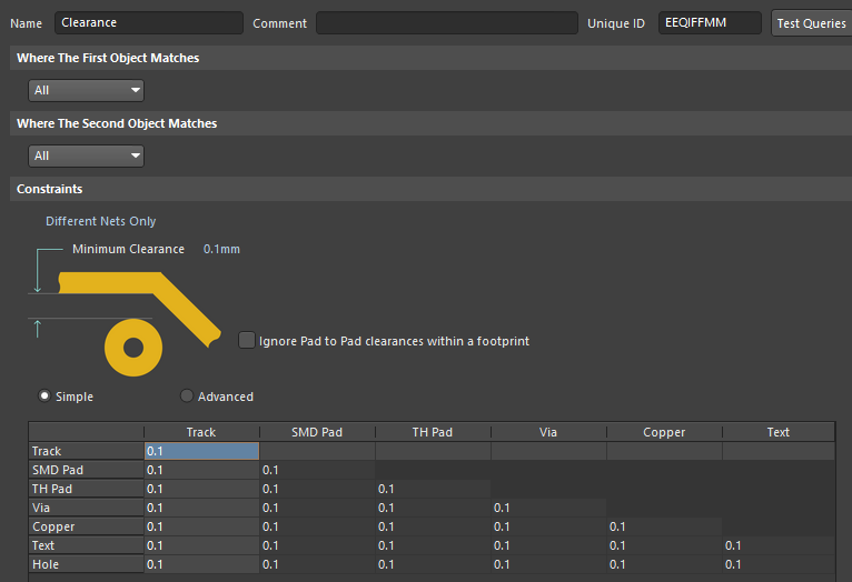
Click Apply at the bottom-right of the dialog to save the settings. In addition to the clearance rules, the Electrical region allows you to configure the rules for Short-Circuit, Un-Routed Nets/Pins, Modified Polygons, and Creepage Distance. These rules are not required within the scope of this guide.
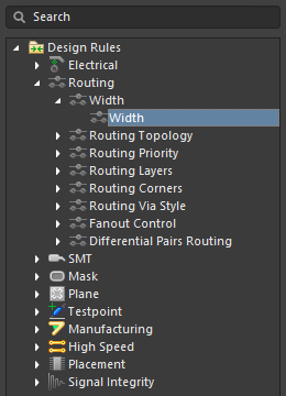
Now we will configure the mandatory Routing rules.
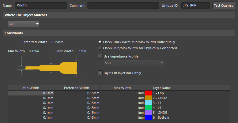
Expand the Routing region. Let’s configure the Width rules. Expand the Width sub-region then select Width.
The constraint manager for all traces of our project is displayed. You can set minimum, preferred and maximum widths for every layer of your PCB. Common traces of our drone PCB should be routed with 0.15mm width and shall not exceed 1mm and be less than 0.1mm, so set Min Width to 0.1mm, Preferred Width to 0.15mm and Max Width to 1mm as shown below.
Previously, we created a separate Net Class containing power nets. Now it’s time to add another width rule that will only work on the Net Class we created. Right-click on the default Width rule then select New Rule from the context menu.
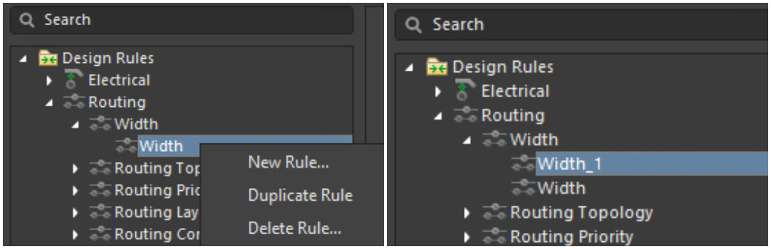
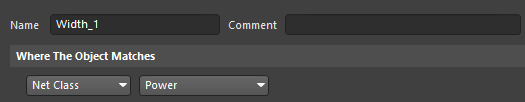
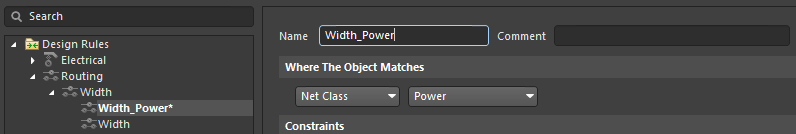
Open Width_1. We need to limit the rule to the Net Class we created earlier. Click the drop-down menu in the Where The Object Matches region then select Net Class. In the right-hand drop-down, select Power. This selection limits the applicability of the rule to one net class.
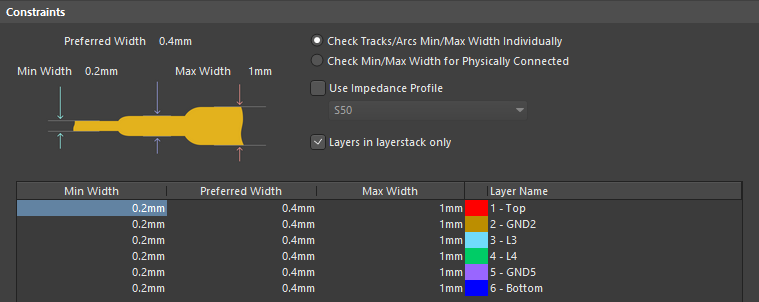
Currently, default values are set for Min Width, Preferred Width, and Max Width. Set Min Width to 0.2mm, Preferred Width to 0.4mm and Max Width to 1mm.
Our rule has the default name Width_1. Since we have only two rules, we can remember that this rule is responsible for the width of a separate net class, but how do you keep track of the rules when there are several more? Renaming the rules at this stage will significantly increase the understanding of the rules in the future. You can specify the rule name in the Name field when the rule configuration window is open. Enter the name Width_Power in the Name field. Click Apply at the bottom of the dialog to save the rule.
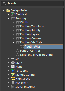
Now we need to set the range of allowed vias for our PCB. Expand the Routing Via Style sub-region then select RoutingVias.
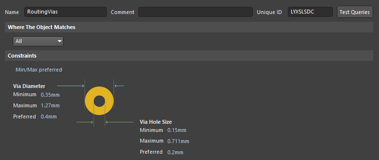
Let's assume the company that will manufacture our PCB can execute the minimum via hole size at 0.15 mm and via pad at 0.1 mm (0.15mm/0.35mm), however, the main via size will be 0.2mm/0.4mm. Define the Minimum Via Diameter as 0.35mm, the Preferred Via Diameter as 0.4mm, the Minimum Via Hole Size as 0.15mm, and the Preferred Via Hole Size as 0.2mm. Click Apply to save the rule.
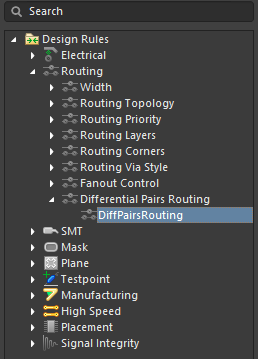
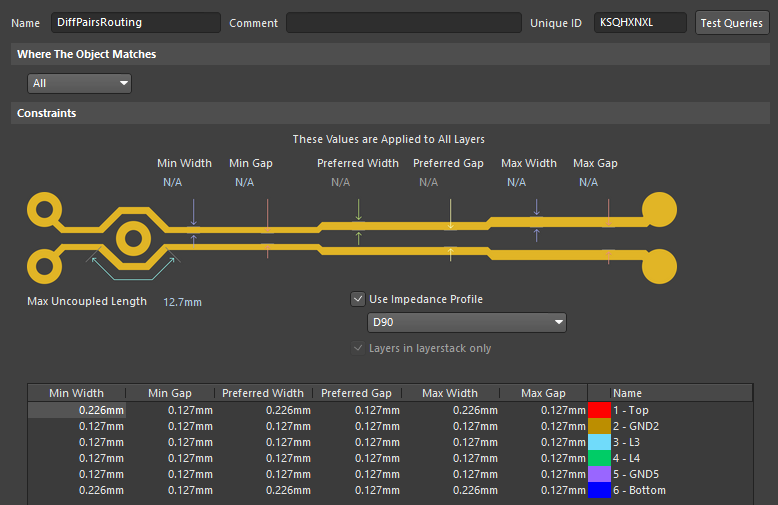
Our PCB design implies the use of a differential pair. It is known that separate requirements to impedance are applied to a differential pairs routing, so we need to configure it. There is only the USB_P/N differential pair so our rule will be set for all differential pairs. Expand the Differential Pairs Routing sub-region then select the DiffPairsRouting rule.
As part of the creation of the PCB stackup, we created an impedance profile for differential nets with 90 ohms impedance. Now we can use it for instant differential pairs configuration. Enable the Use Impedance Profile option in the Constraints region. The width values will be updated based on the specified impedance. That’s all there is to it! Quick and easy, right? Click Apply to save the rule settings.
The next mandatory step is to specify the size of the solder mask expansion and the solder paste indent.
Expand the Mask region, expand the Solder Mask Expansion sub-region then select SolderMaskExpansion.
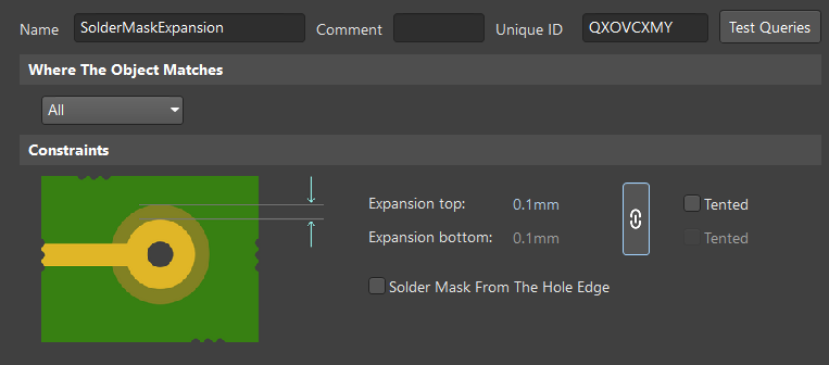
Set Expansion top to 0.1mm. Make sure that the link between the Expansion top and Expansion bottom expansion is enabled as shown below (click to enable/disable). Click Apply to save the rule configuration.
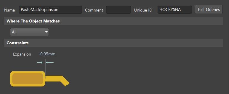
Expand the Paste Mask Expansion subsection then select PasteMaskExpansion.
Set Expansion to -0.05mm. In order to improve the solderability of the components, it is recommended to set the paste expansion smaller than the pad size. Click Apply to save the rule configuration.
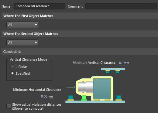
The last step in configuring the mandatory basic rules for the current project is to specify the component placement rules, specifically, the rule of vertical and horizontal clearance between the components. Our PCB is a part of a multi-board assembly and any miscalculation in the design of a single part of the device endangers the final assembly and operability of the entire unit. Let's create the rule.
Expand the Placement region. Expand the Component Clearance sub-region then select ComponentClearance.
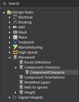
Set Minimum Horizontal Clearance to 0.05mm and the Minimum Vertical Clearance to 0.1mm. Click Apply to save the rules. Close the PCB Rules and Constraints Editor dialog. Our work is done here.