Differential Pairs Routing
In our drone's PCB, there is a USB differential pair that also needs to be routed. Routing of differential pairs is similar to routing single traces but uses a separate tool named Interactive Differential Pair Routing. You can access this tool using the Active Bar or by selecting Route > Interactive Differential Pair Routing from the main menus. Let’s route our differential pair.
Choose Route > Interactive Differential Pair Routing from the main menus. We need to start routing from pins 70 and 71 of the U12 component. Click on either of the pins to start differential routing.
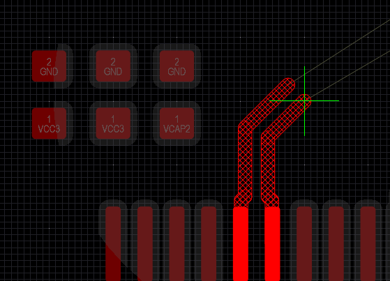
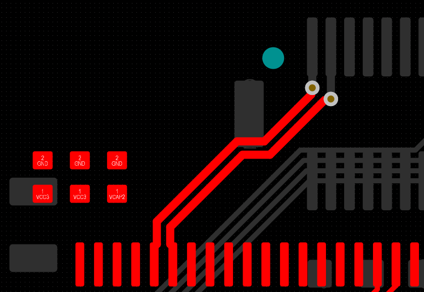
We need to connect this differential pair to the CN1 component located at the bottom of the PCB, so make a via transition using the - on the number keypad. The completed differential routing is shown in the figure below.
For your routing to be perfect, there are basic rules that will help you avoid signal integrity problems.
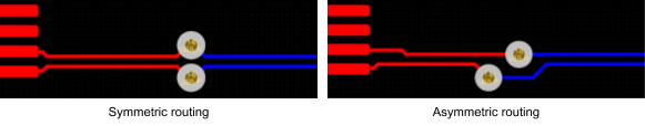
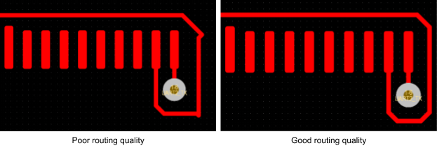
- Differential pairs should be routed as symmetrically as possible relative to each other. Any divergence in symmetry breaks the tracks coupling, leads to impedance discontinuity, and negates the differential pair usage benefits. Wrong tracks can be moved taking this rule into account or retraced if necessary.
- Avoid straight and sharp angles during track placement. It is highly recommended to use 45 degree angle routing mode. Incorrectly angled tracks cause negative changes in signal quality. This can be easily corrected by using the Gloss feature. Select the entire track then choose Route > Gloss Selected from the main menus to automatically improve the route quality for the placed track by reducing the overall length and number of corners. You can also place the new track above the already placed track to replace it with the new routing style.
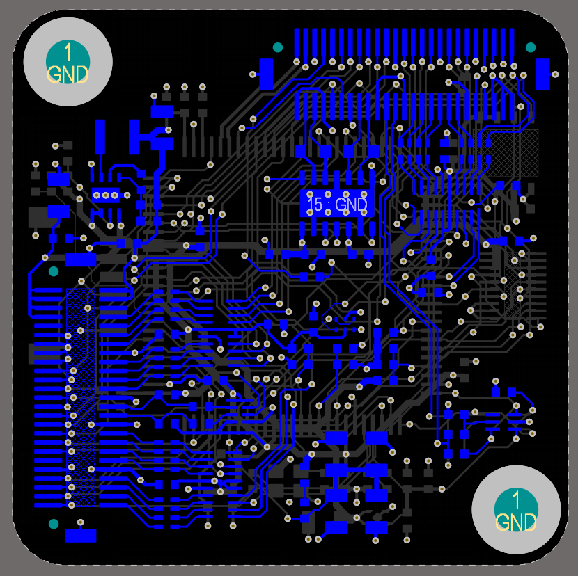
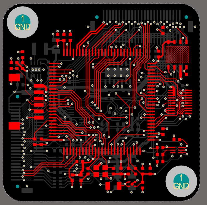
You now have all the basic skills you need to finish the routing of this PCB. Show your imagination and complete the routing. Don’t forget to use the Show/Hide connections option. If you have difficulties, you can refer to the figures below. Don't worry if you cannot connect all the GND pins as they will be connected by a polygon in the next chapters.
![Completed routing for Inner Layer 3 [3] L3](http://files.my.altium.com/sites/default/files/inline-images/image4_11.png)
![Completed routing for Inner Layer 4 [4] L4](http://files.my.altium.com/sites/default/files/inline-images/image3_12.png)