

Efficient Routing Control
Track placement is the basis for all work on the PCB design. An important part of understanding the interactive router is to first understand how connectivity is managed in the PCB editor. When the design is transferred from the schematic, the components are placed onto the PCB workspace and the connection lines are displayed, indicating which pads connect to each other in each net.
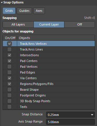
First, let’s configure snapping for automatic attachment of tool crosshairs to different PCB objects. This option will help you avoid mistakes by ensuring the trace is connected precisely to the necessary objects.
Open the Properties panel then expand the Snap Options region. Select Current Layer in the Snapping region. This means that the snapping will only work for the active layer. Enable Track/Arcs Vertices, Intersections, Pad Centers, Via Centers, and Regions/Polygons/Fills in the Objects for snapping region. Enter 0.25mm for the Snap Distance.
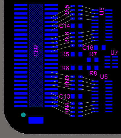
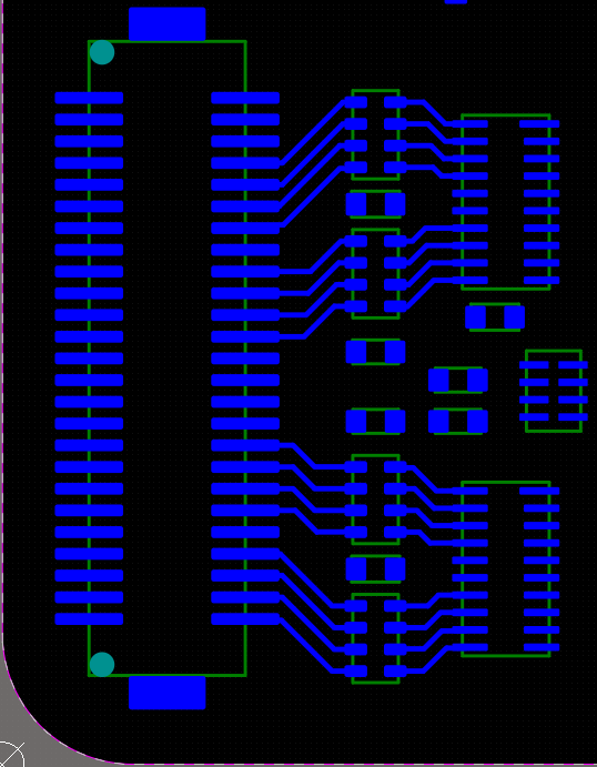
Make the Bottom Layer active. Let's make some adjustments to the visibility of the necessary connections between the components as an unrouted board can appear intimidating as a mass of connection lines crisscrossing all over the board. First, we need to hide all connections. Press the N button to open the Connection Visibility pop-up menu then select Hide Connections > All. Now all connections are hidden. We need to turn on connection visibility for certain components on the bottom side of the PCB. Press N again then select Show Connections > On Component then click on the RN3-RN6 components. Right-click to exit the command. The connection lines are now displayed only for those components.
Choose Route > Interactive Routing from the main menus. After launching the command, click on a pad from which you want to start routing. Click on the top left pin of the RN5 component to start routing. Make sure that the track width is equal to 0.15mm. Route your track to the pin of the CN2 component as shown below.
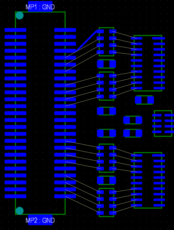
While routing, you can toggle the corner direction by pressing the Spacebar. Click to place a fixed segment. After clicking, you will see that the fixed segment has a solid fill and the ‘unfixed’ segment has a grid fill. When you move the mouse, only the unfixed segments will change. This allows you to build a trace on any path you want.
Finish the routing for all connections as shown in the figure below.
The era of single-layer PCBs is long gone. Now the majority of PCBs are designed with several internal metal layers. These boards are called multi-layer boards. As you will recall, we created a PCB stackup with six layers - this set of layers is minimal for the proper placement of signals. The connection between the layers is provided by vertical inter-connection access (or via) and are presented as a drilled metalized hole in the PCB. Let’s connect some signals through layers.
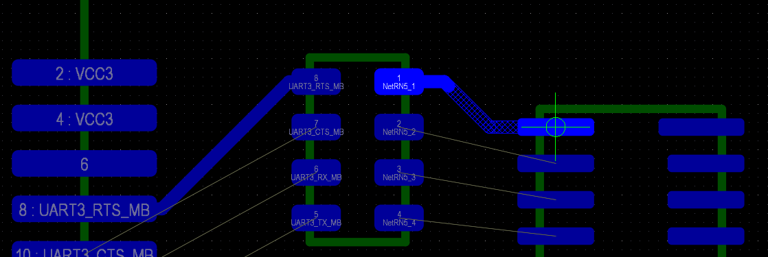
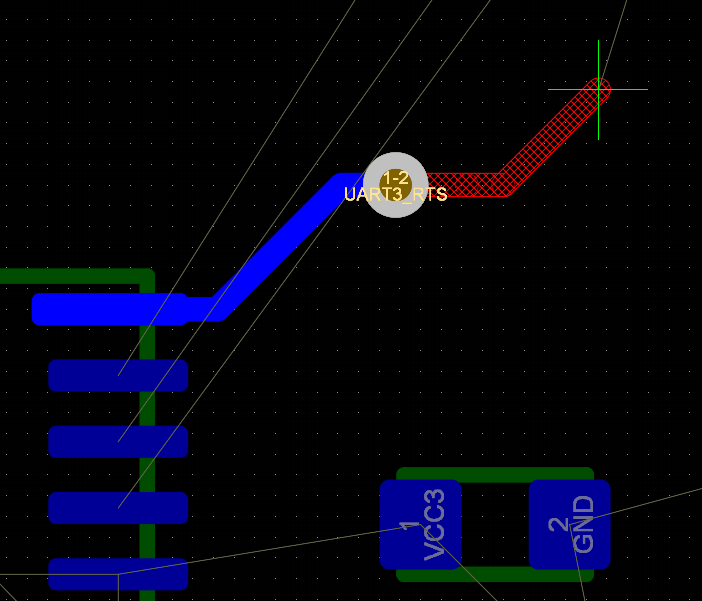
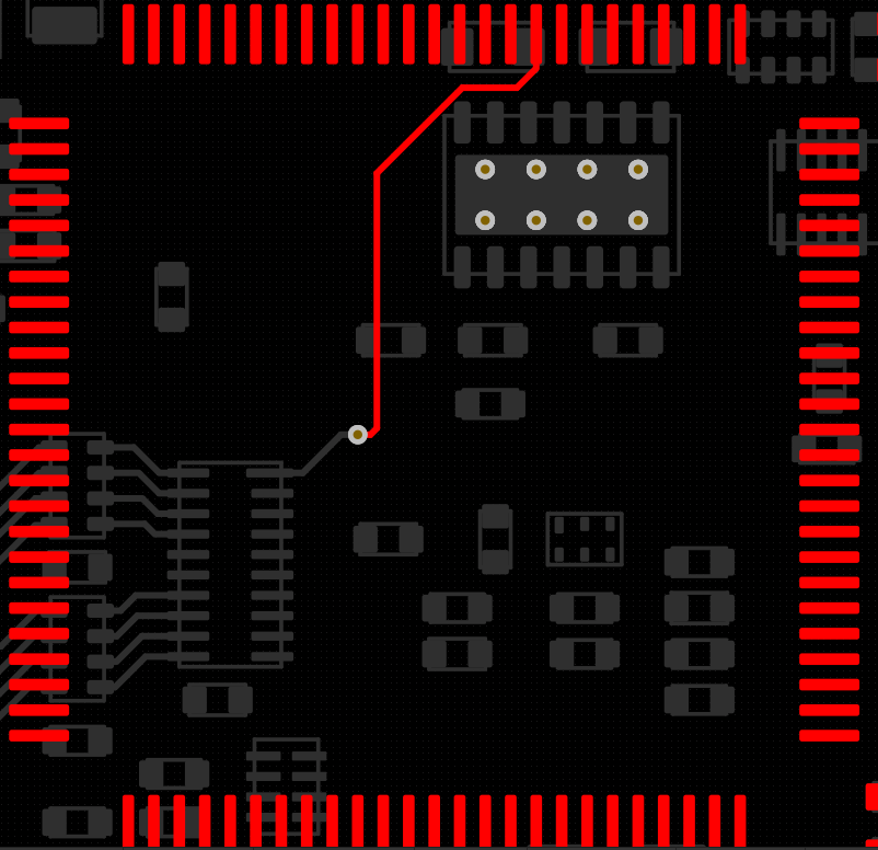
Turn on the connections visibility for the U6 component then run the Interactive Routing command. Click on pin 1 of the U6 component to start routing. We need to route the UART3 signal group to the U12 component that is placed on the top side of the PCB. Route a track as shown in the figure below then press + on the number keypad to make the via transition to the next layer (Bottom > Top). Finish track placement as shown below.
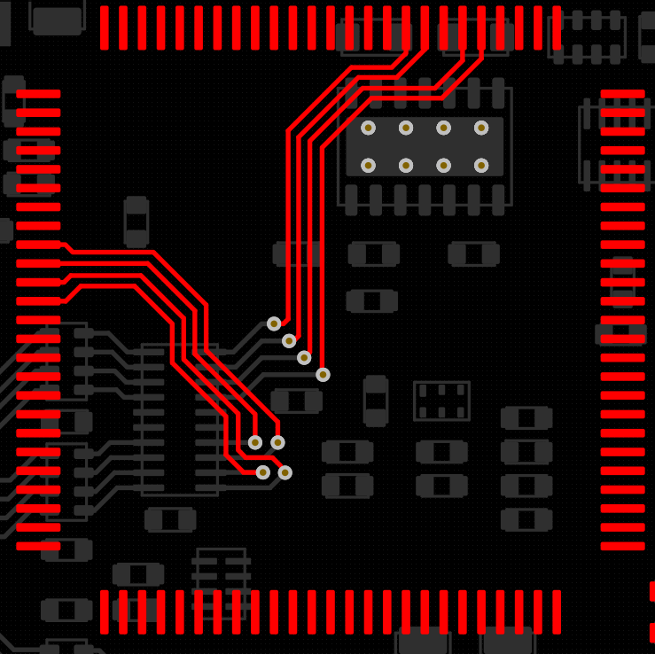
Route the UART2 and UART3 signal group. The figure below shows the correct placement of vias and tracks.
Our PCB consists of six layers (of which two are reference planes).
Let’s put a signal group on the inner layer.
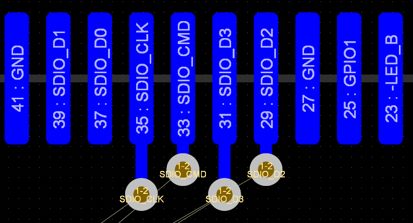
Find the CN1 component on the bottom side of the PCB. Press N, select Show Connections > Net then click on pins 29, 31, 33, and 35.
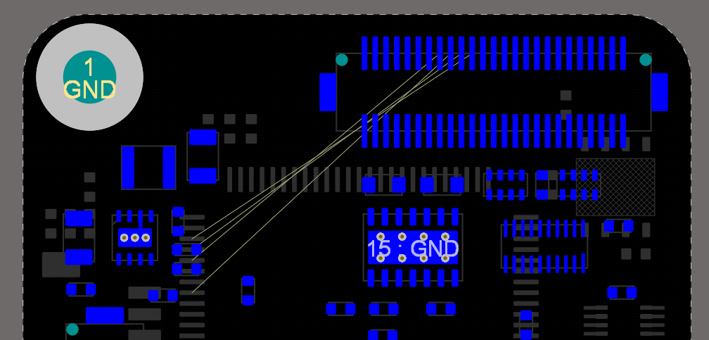
In the next step, we will make a repetitive fanout pattern for this component.
Run the Interactive Routing command. Starting from pin 35, route a small track segment and place a via. Afterward, make a smaller track for pin 33 and place a via as shown in the figure below. The configuration of these tracks will become a via pattern for this component.
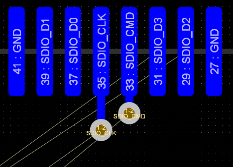
We need to repeat this fanout combination for adjacent pins 31 and 29, which can easily be done using the Copy/Paste feature.
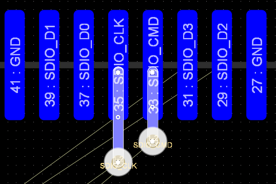
Select both placed vias. Press the Tab key to select the entire net in this layer.
will be copied in the next step.
Press Ctrl+C to copy the selection. A crosshair will appear, which will select the anchor point of the copied object. Click on the center of pad 35 to define it as an anchor point. (Ensure that the snapping circle has appeared before clicking.)
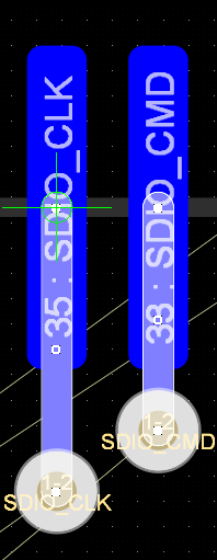
Press Ctrl+V to start pasting. Copied objects are now attached to a crosshair and they are ready to be placed. Also, notice that the object's position that is attached to the crosshair is identical to the anchor point selected in the previous step. Click on pin 31 to place the fanout pattern. After placement, the copied objects are updated with new net names according to the pins.
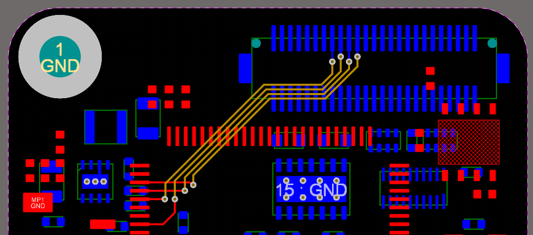
This signal group will be routed in the Inner layer [3] L3, therefore, make this layer active. Route signals in layer L3 to the necessary pins of the U12 component. Refer to the figure below as an example.
These are the main approaches to placing tracks and vias on a printed circuit board. The next chapter describes the nuances of differential pair placement.