Silkscreen Placement
All drawings and designations on the PCB are realized with silkscreen printing. With the help of silkscreen, you can mark each component: its designator, borders, part number, and first pin position. Additionally, you can add any objects to other objects, such as a project name, a company logo, the developer's initials, etc. Silkscreen printing also helps to significantly simplify final product assembly since all the information for the assembler is on the PCB. All component designators are already present in the drone PCB as they were transferred during the first project synchronization. Altium Designer has Top Overlay and Bottom Overlay layers that are used for silkscreen. Any primitives on these layers will eventually be applied to one of the external sides of the board during production. Let's create a silkscreen for the PCB.
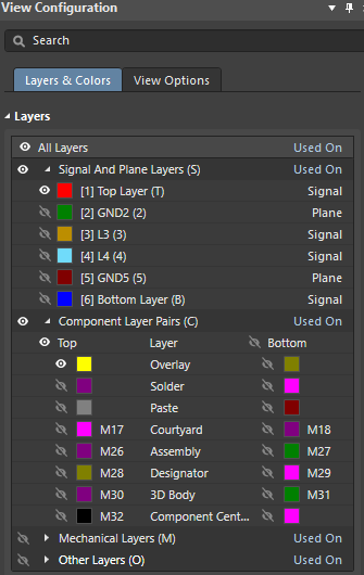
Open the View Configuration panel. Make the Top Layer and Top Overlay layers visible. When setting up the Top Layer silkscreen, it is recommended that you use this configuration to prevent silkscreen objects from reaching the component pads.
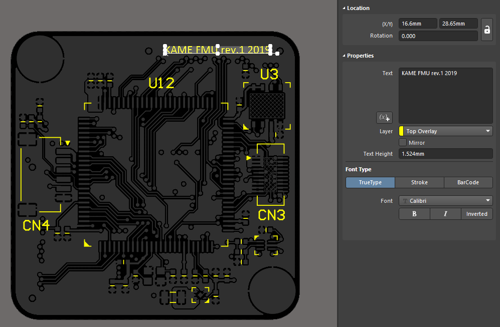
For the Top Overlay layer, let's mark the largest and most important components: U12, U3, CN3, and CN4. We will hide designators for all other components. To do this, make the Top Layer active, select only Components in the Selection Filter region of the Properties panel in Board mode then select all components on the PCB using right-to-left selection. While holding the Shift key, deselect the components listed above. In the Properties panel in Component mode, click on the visibility icon next to the Designator field in the Properties region.
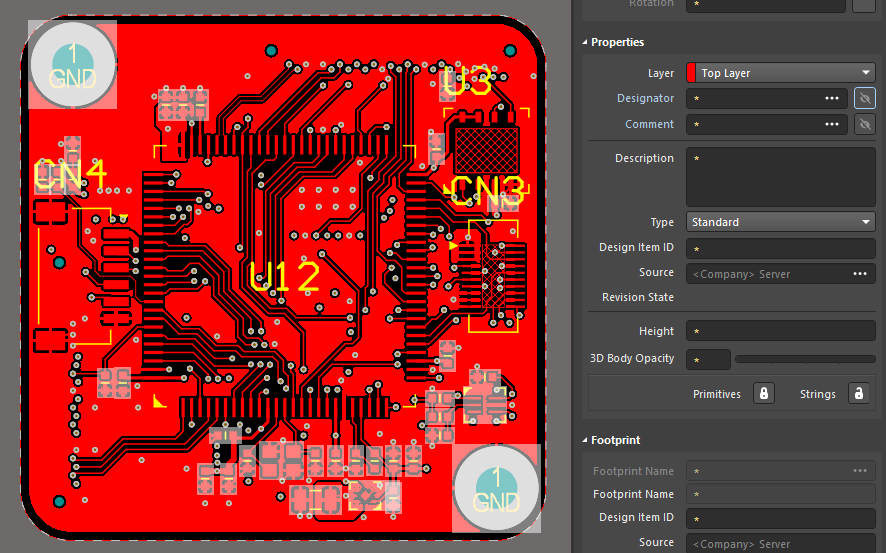
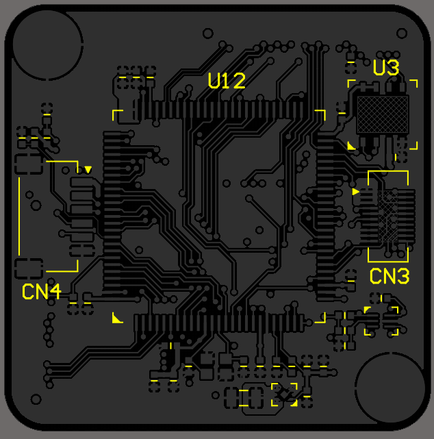
Make the Top Overlay layer active and dim the Top Layer by pressing the Shift+S key combination. Now, let’s place the designators of these components so that they appear neatly on the board and do not cover the component pins. Activate Texts in the Selection Filter of the Properties panel. You can move and place designators, but it is recommended to decrease their size. Select all Designators then set the Text Height to 1mm in the Properties panel. Also, define the Stroke Width as 0.2mm in the Font Type region. Place designators as shown in the figure below.
Let’s add custom text to our PCB. Choose Place > String from the main menus to begin text placement. Press the Tab key to pause placement so we can configure the text string before placement. Enter KAME FMU rev.1 2019 in the Text field in the Properties panel then select TrueType as the Font Type, and select Calibri from the Font drop-down menu. Place the text string as shown in the figure below.
Now let’s do a silkscreen for the bottom layer. Open the View Configuration panel and deselect the Top Layer and Top Overlay layers. Make the Bottom Layer and Bottom Overlay layers active. As you can see, all component designators for the bottom layers are mirrored. This is the correct display of the designators for the bottom side, so there is no need to change the Mirror option in the Properties panel. For convenient interaction with designators on the bottom PCB side, flip the board upside down by pressing the Ctrl+F key combination.
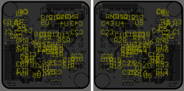
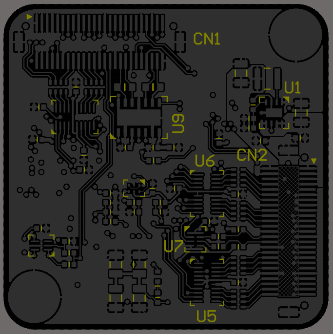
Using the above approach, mark the CN1, CN2, U1, U5, U6, and U7 designators on the bottom side of the PCB. The result should look similar to the figure below.