Configuring Advanced Design Rules
Configuring the Polygon Rules
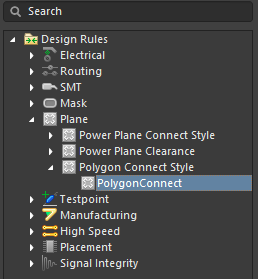
The next step is to configure the Polygon Connect Style. Expand the Plane region, expand the Polygon Connect Style sub-region then select PolygonConnect.
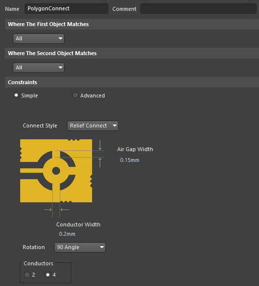
Make sure that the Connect Style drop-down is set to Relief Connect. Set Air Gap Width to 0.15mm and Conductor Width to 0.2mm. Click Apply to save the rule.
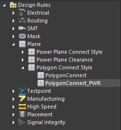
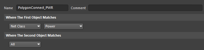
We need to also set a separate connection rule for the polygons that will belong to a power net class, as this net requires direct vias connection. Create a new rule by right-clicking on Polygon Connect Style then select New Rule from the context menu. Click PolygonConnect_1 then change the Name to PolygonConnect_PWR.
This rule will define the parameters of the polygon’s connection to different types of pins that belong to the Power net class. To start with, let's configure this rule so that it applies only to objects of the Power net class. In the Where The First Object Matches region, select Net Class from the first drop-down menu then select Power from the second.
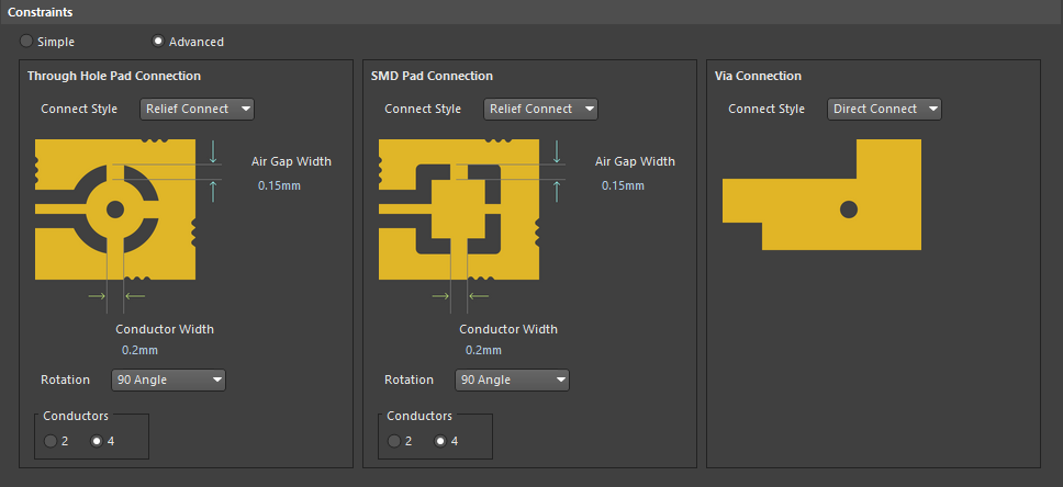
When working with plane or polygon rules, you can set simple or advanced rules for plane/polygon connections by choosing either Simple or Advanced in the Constraints region. The Simple rule configuration offers a common connect style for all types of pins and vias. The Advanced rule configuration is more flexible and allows you to customize the connection style for each pin type. Select Advanced. Three types of connection styles are available. In the Via Connection region, use the drop-down to set the Connect Style to Direct Connect so the future via polygon stitching and all via transitions will not break polygon integrity and will maintain proper copper balance. In the Through Hole Pad Connection and SMD Pad Connection regions, set the Conductor Width to 0.2mm and Air Gap Width to 0.15mm.
Click Apply to save the changes.
Configuring the Manufacturing Rules
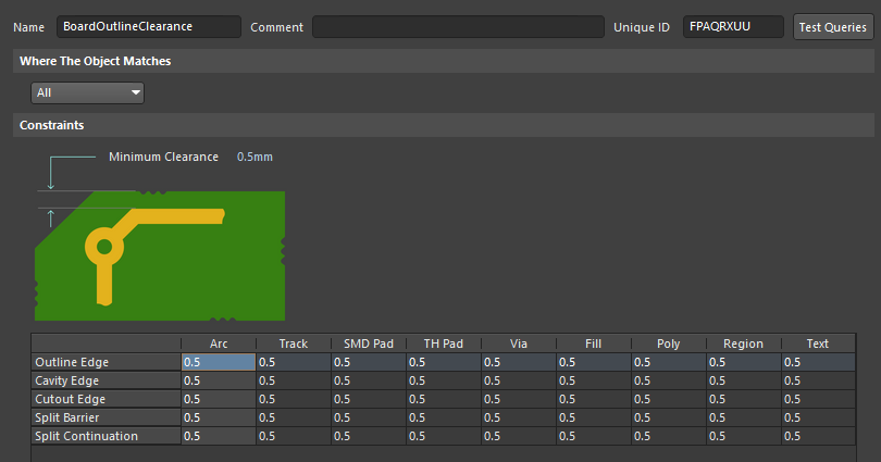
We need to form an offset from the board shape contour to avoid PCB production errors.
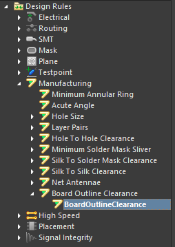
Expand the Manufacturing region. Select the Board Outline Clearance sub-region then create a new rule named BoardOutlineClearance.
Set the Minimum Clearance to 0.5mm. Click Apply to save the rules.