

Searching for Errors
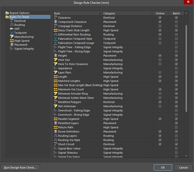
You have already worked with the enable Online option in the Design Rule Checker dialog, which showed certain errors in real-time. However, you should be aware that the online DRC with the default settings does not check all errors and you should definitely do a full check of DRC design rules. Also, some errors may not be checked for Batch DRC checks. You can enable or disable Batch and/or Online checking of specific rules by selecting Rules To Check in the Design Rule Checker dialog.
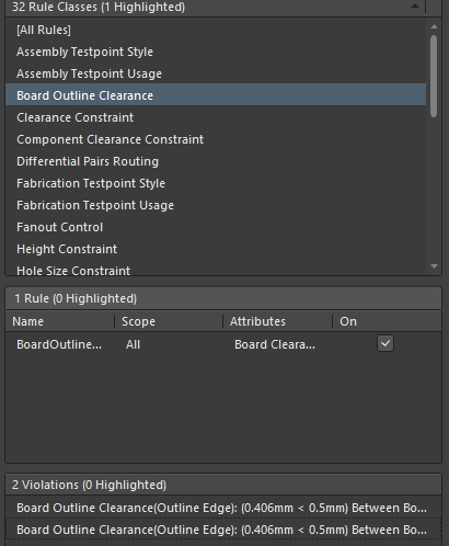
Once the full DRC check is completed, you should have at least two violations related to the Board Outline Clearance rule. This chapter will show you the most convenient approach to correctly localize and fix all the violations.
Open the PCB document or select its tab. You can easily and conveniently interact with all violations using the PCB Rules And Violations panel. Click the Panels button at the lower-right corner of the workspace then select PCB Rules And Violations. The panel provides a central point for browsing and editing rules, initiating design rules checks, and viewing individual violations as graphic overlays in the design space. It is recommended to place this panel with the left panel group (with the Projects panel and PCB panel) for an organized work environment.
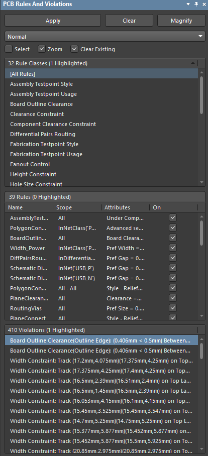
The upper region of the panel lists all classes of rules in which errors may have been made. You should pay special attention to the following classes because they usually contain critical violations:
- Clearance Constraint
- Component Clearance Constraint
- Differential Pairs Routing
- Height Constraint
- Hole Size Constraint
- Hole To Hole Clearance Constraint
- Net Antennae
- Short-Circuit Constraint
- Un-Routed Net Constraint
- Width Constraint
There should be no violations in the above-listed classes!
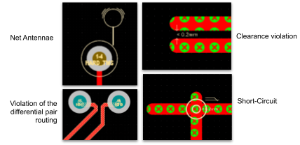
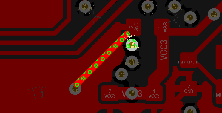
All errors on the PCB are visually marked by a special pattern and/or special symbol indicating the violation
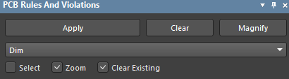
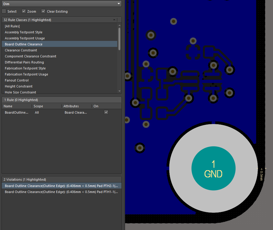
The controls in the upper region of the panel are used to control the visibility of a violation when it is selected in the list. In the drop-down menu, select Dim (instead of Normal). When the Dim option is selected, all other objects will be dimmed when the violation is selected in the Violations list leaving the focus on the object with the violation. Also, enable Zoom to zoom the selected violation and Clear Existing to remove selection/dimming after the selection of another violation.
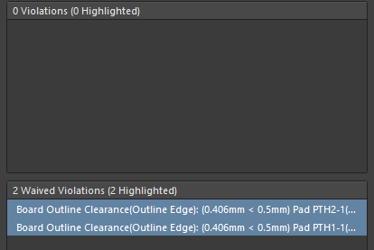
With the rules we have set, we have at least two violations related to the Board Outline Clearance. Click the Board Outline Clearance class in the PCB Rules And Violations panel to see all related errors. After selecting a rule class, the regions below will show the rules related to that class (Rule(s)) and a list of all objects that violate this rule (Violation(s)). Each violation has a brief description of the violation of the rule. In this case, the PTH1 and PTH2 mounting holes are placed 0.406mm from the edge of the PCB, but the BoardOutlineClearance rule specifies a minimum gap of 0.5mm.
Click one of the violations to highlight it on the PCB. As you can see, the design space zoomed in to the violating object and highlighted it. Now we can perform actions with this object to fix the error.
There are a few approaches to solving violations:
- Change the object so that it will adhere to the specified rule. For example, if there is a clearance violation, move the violating object away from the adjacent object.
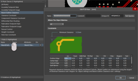
- Change the rule so that the object will match it. For example, if the specified rule is too strict, you can lessen the restriction of the rule. You can quickly navigate to the required rule by double-clicking it in the Rule(s) region of the panel.
- Waive a violation. There are times when objects on the PCB are placed with rule violations deliberately, but the DRC system will highlight them anyway. If you are sure that there are no violations with these objects and the rule violation was caused by the peculiarities of the design, you can waive a violation.
In the case of the mounting holes violations, the violation of the rules was done deliberately, so we will waive those violations.
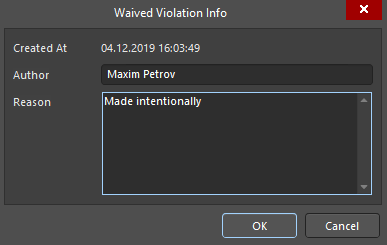
Select both violations related to mounting holes by clicking them while holding the Ctrl button. Right-click on one of them then select Waive Selected Violations. The Waived Violation Info dialog opens, which contains information about the current date, the author and the reason why the violation is waived. In the Reason field, enter Made intentionally then click OK to waive violations.
After waiving the violations, a new region titled Waived Violations appears in the PCB Rules And Violations panel. In this region, you can review all waived violations, view the reason and, if necessary, ‘unwaive’ them.
Fix all violations of the Rules Classes specified in Step 1 without changing the rules or waiving violations. If you have any other errors, the next chapter will review the most popular errors with approaches to fixing them.