

Placing a Custom 3D Body in 3D View
The 3D view allows you to see the results of your work as if it was real. With the help of the 3D view, it is possible to view a PCB design from all sides, to check on component placement, silkscreen alignment, and many other visual aspects directly related to the appearance of the final product. Altium Designer also allows you to load and place a 3D model of a previously created .sldprt or .step file in the design space and to evaluate the correct placement of the mounting holes, the component’s height, the absence of interference between the board, and, if necessary, to make changes to the design at an early stage of development. Let's add a 3D model to our project.
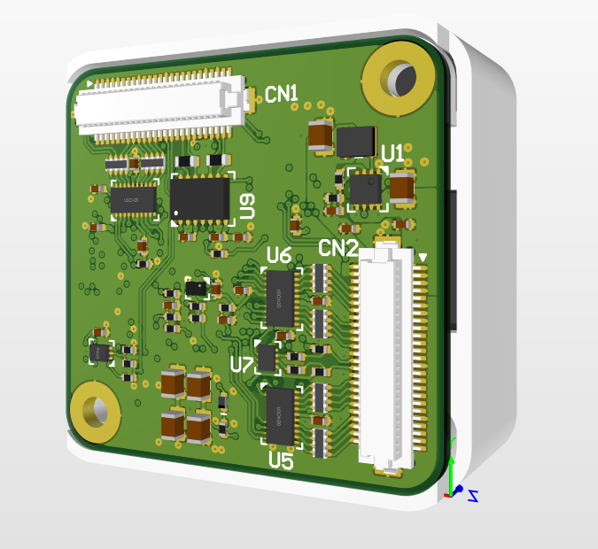
Press the 3 key to switch to 3D viewing mode. You can also use the 3D Off/On option on the View Options tab of the View Configuration panel. The board we created is now displayed in 3D mode. Note that after switching to 3D mode, the contents of the View Configuration panel have changed. There is now a Projection display choice of either Orthographic or Perspective, a Show 3D Bodies Off/On option, and a list of the PCB materials (copper, core, silkscreen, and solder mask) with the ability to edit the color and transparency of the materials to create the view configuration you require.
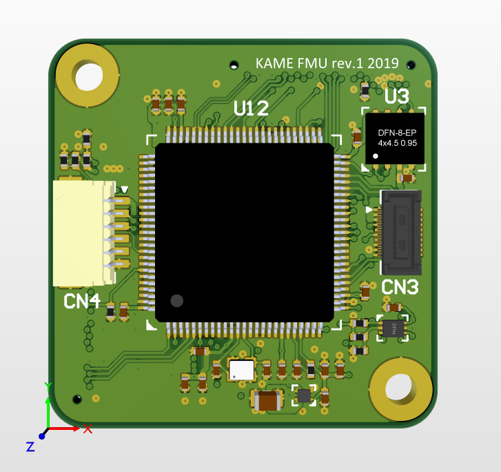
The 3D model can be easily tilted and rotated to display it from different angles. If you've worked in 3D editors before, you'll be familiar with the basics of camera control.
To move the camera along a single axis, right-click and hold then move the mouse; the camera will move with the movement of the mouse.
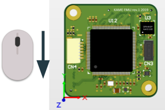
To zoom in, click on the mouse wheel and move the mouse up while holding down the wheel.
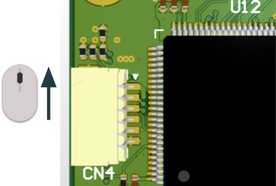
To zoom out, repeat the above procedure except move the mouse down while the wheel is pressed.
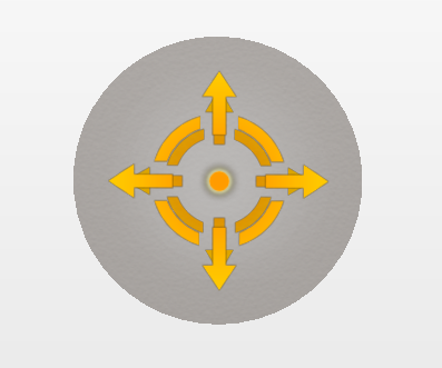
Press the Shift key to display the navigation ball. When the Shift key is held down, you can tilt and rotate the camera either in free mode (the first right-click should be made without touching the arrows or arcs of the navigation ball) or on one specific axis (the first right-click should be made on one of the arrows or arcs inside the navigation ball). You can also quickly flip the PCB using Ctrl+F.
Altium Designer allows you to load any 3D models of housings, plates, holders, panels, screws, etc. In other words, you can place anything that can help you design and customize the construction for your PCB. Let's add a housing element to the design space that is tied to the design of our PCB. Before starting, download this 3D model file and place it in a convenient location.
Select View > Zero Rotation from the main menus to reset the camera rotation. Make sure the camera is facing the PCB top side as shown in Fig. 1. Select Place > 3D Body from the main menus to run the 3D Body placement tool. In the window that opens, select the downloaded 3D model Kame-FMU-Case.step then click Open to start the model placement.
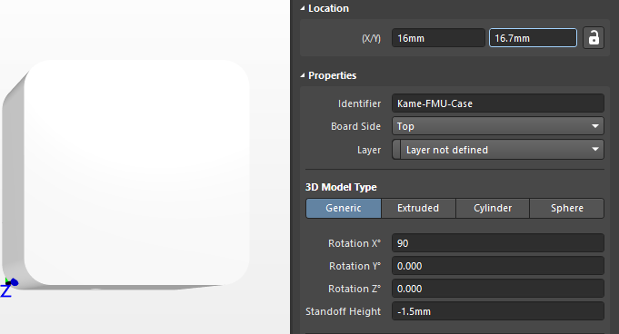
After clicking Open , the selected 3D model will be attached to the mouse cursor. Press Tab to pause the placement so that we can configure the model rotation and standoff height in the Properties panel. Define Rotation X as 90 degrees and Standoff Height as -1.5mm . Press the Tab button again to continue the 3D model placement. Place the 3D body by clicking anywhere on the design space then right-click to exit placement. We will configure the proper placement by using coordinates in the next step.
Select the placed 3D model (3D Bodies should be active in the Selection Filter region of the Properties panel). Define its X/Y coordinates in the Location region of the Properties panel as:
X: 16mm
Y: 16.7mm
You can also change the color of the model and its opacity in the Display region of the Properties panel. Enable the Override Color option then define the color as gray. Change the Opacity to 50%. Click in any empty space to reset the selection.
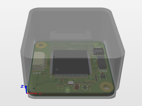
There is still a lot of free space in this construction. In the future, there will be a rigid-flex PCB that will be connected to the CN4 connector. At this stage, the placement of the 3D model for our PCB is complete. After saving the project, the 3D model will remain. Also, the rules of horizontal and vertical clearance will be applied to this 3D model, so you will be able to change either the design of the housing or the placement of the components. You can place the 3D model in the very first stages after you have defined the board shape, in which case you will be able to initially design the board to suit your housing.