Setting the New Standard in Electronics Design.

Efficiency. Collaboration. Accuracy.

Switch and Get the Power to Design Without Limits

Get 50% off when you switch to Altium Designer before April 30, 2024

Create Your Own PCB / Board Shape Import Using a DXF/DWG Drawing Completed Sign In To Save Your Progress
Click if you find this content useful

Create Your Own PCB

Board Shape Import Using a DXF/DWG Drawing

Now that we have created a PCB document, the most interesting and creative part of the development cycle begins - the creation of a printed circuit board. The PCB creation process is quite complicated and time-consuming, however, with the modern tools in Altium Designer, the process is much easier and faster. Even the biggest endeavors start with a small step; the first step in PCB creation is to define the contour of the board. There are several ways to create your own board shape as you will learn in this guide.

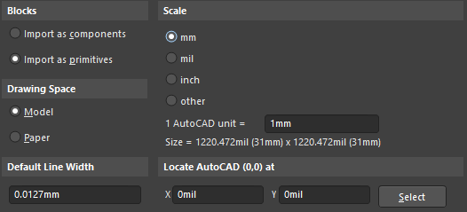
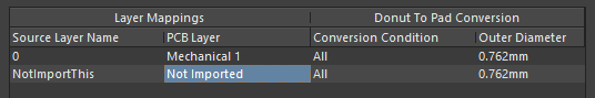
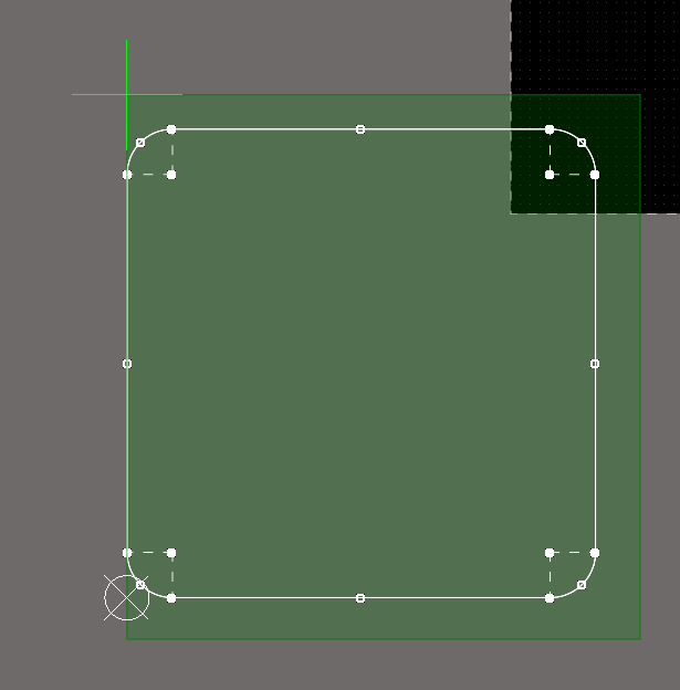
The recommended way to create a board shape is to use a contour import from MCAD systems. This shape must be created earlier and uploaded from your favorite CAD system in DXF or DWG format. Before uploading, check your shape in MCAD - it must be completely closed, otherwise, the board shape will not be applied! Within the scope of this guide, use the DXF file attached in step 1. Let’s get started.

Download this file to any location you prefer. This is a DXF drawing that will be imported as a board shape.  
Make sure that you have your PCB document open and activated. Select File > Import > DXF/DWG from the main menus. Select the previously downloaded DXF file in the File Explorer window that opens then click Open. The Import from AutoCAD dialog will open.
Initially, the drawing was created in the millimeter unit system, therefore, it is necessary to choose that format. In the Scale region, select mm. The board size now displays 31x31mm.
Fig. 1 - Scale unit selection
Now we need to configure the layer mapping so that the source DXF layer will be imported as a mechanical layer. We have two layers in the DXF file - the default 0 layer, which contains the board shape contour and the NotImportThis layer. The DXF layers mapping to project layers is set in the Layer Mappings region. Click on the name of the layer in the PCB Layer column to set the matching then click the ▼ symbol to open the layer selection menu. Map the 0 source layer to Mechanical 1 PCB layer; this layer will become our board shape. Set the NotImportThis source layer to Not Imported since we do not need this layer for our design. Click OK in the dialog to proceed with changes. 
Fig. 2 - Required layer mapping configuration

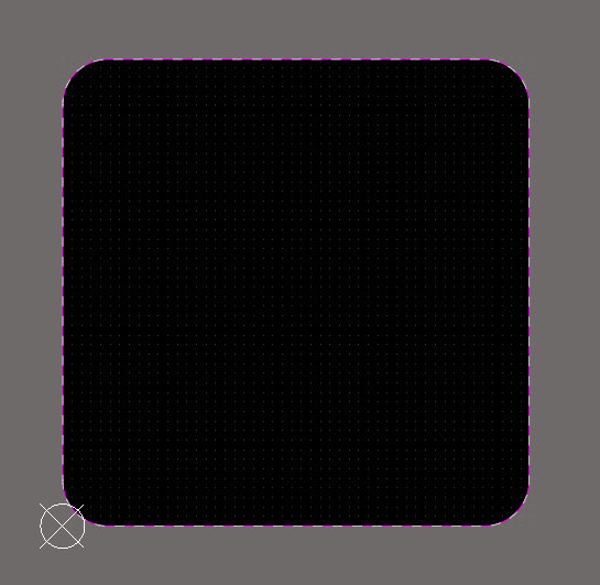
After a successful import, a notification dialog opens stating the import is complete. Click OK to close it. Look at your PCB. A new imported contour with the form of the future PCB has appeared. Let’s define it.

Imported DXF Drawing
Fig. 3 - Imported DXF drawing
Select the entire contour using right to left selection.
Proper contour right to left selection - all primitives are selected
Fig. 4 - Proper contour right to left selection; all primitives are selected

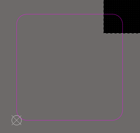
Tip: You can also select the entire contour using another method: select one primitive (line or arc) then press Tab.

Select Design > Board Shape > Define from selected objects from the main menus. The board shape has been updated and now completely replicates the added DXF drawing. 

Re-defined board shape
Fig. 5 - Redefined board shape
Good job! Article is now completed!
Sign In To Save Your Progress

Read Again

CAPTCHA
Was this article useful?
Yes No
Thank you Glad to hear it