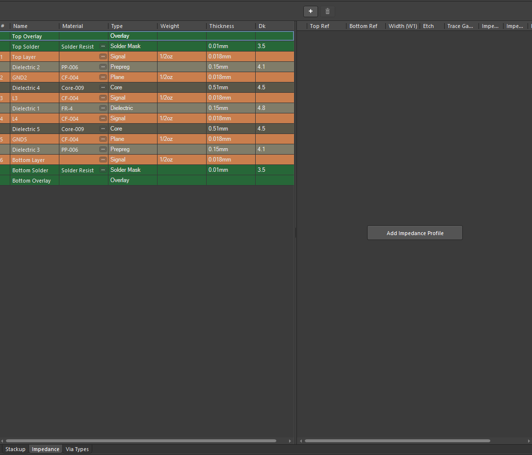
Defining the Layer Stackup
After project synchronization, we are ready to start the development of the printed circuit board. One of the first stages is defining a PCB Stackup. At this stage, we will define the internal design of the PCB that starts with deciding how many metal layers are needed, the PCB thickness, via types, and impedance profiles. During this stage, we need to ask ourselves "will we be able to form an impedance structure with this set of layers?”. If we are able to check with the manufacturer about dielectrics and metallic materials, information about impedance requirements can be found in application design guidelines. With Altium Designer, you don't have to spend a lot of time calculating the impedance profiles and selecting the width and gaps of the conductors and planes. You only need to specify the target impedance; the Layer Stack Manager will automatically select these parameters for you. After that, when working with the rules, you can select the necessary profile for the group of circuits in a few mouse clicks. Let's start forming a PCB layer set!
Stackup Configuration
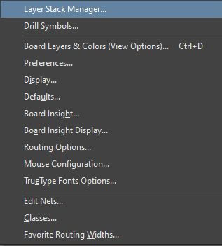
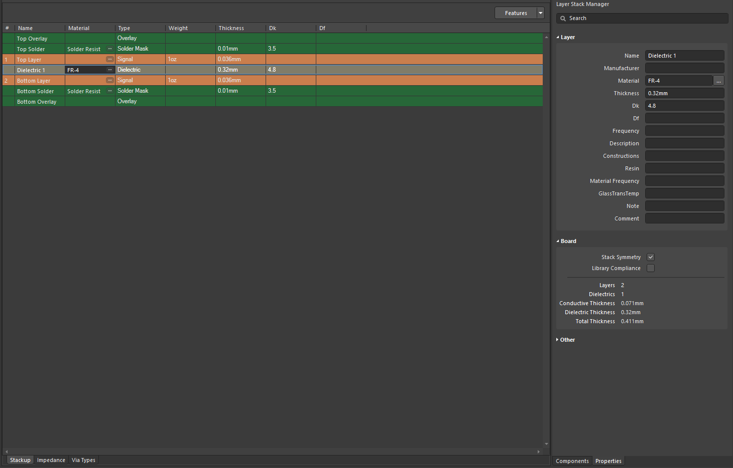
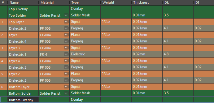
We need to form a layer set for our PCB. Open Kame_FMU.PcbDoc, press O then select Layer Stack Manager. The Layer Stack Manager editor will open in the design space.
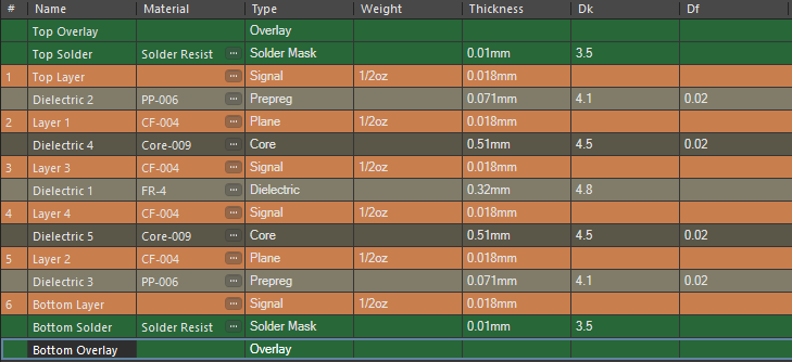
Four layers were added to the PCB stackup (two metal plane layers and two prepreg layers). Using the Stack Symmetry option has automatically balanced the layer set.
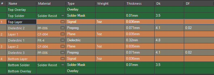

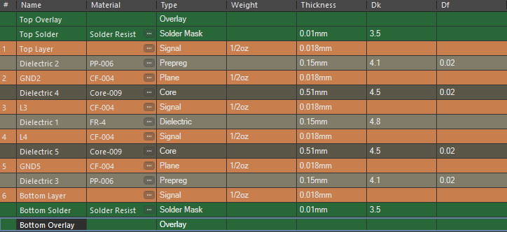
Layer 2 -> GND2
Layer 3 -> L3
Layer 4 -> L4
Layer 5 -> GND5
Your stackup should now resemble the below figure.
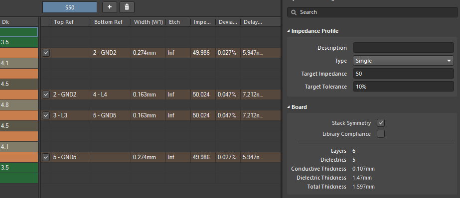
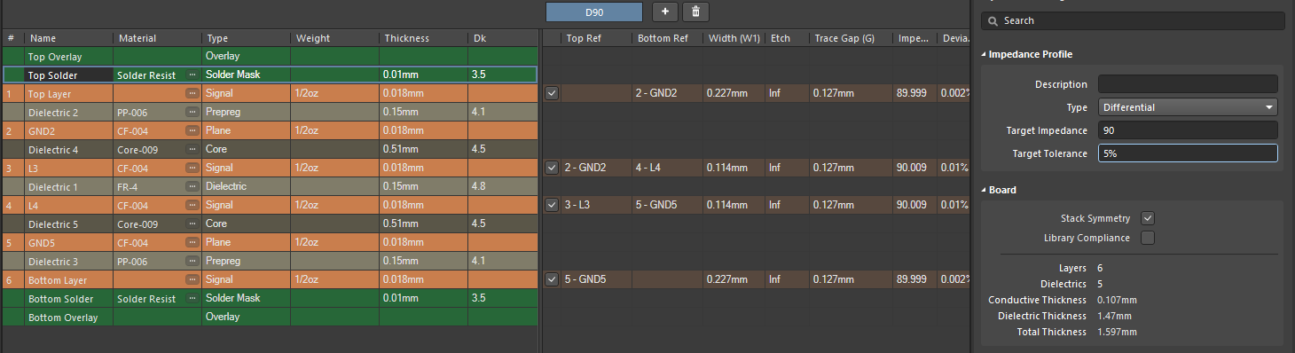
Impedance Profiles
The design of our printed circuit board has a USB interface that requires the placement of differential transmission lines with a 90 Ohm impedance. The Layer Stack Manager allows you to calculate the impedance of the transmission lines as quickly as possible by specifying the target impedance. When you specify the correct impedance value, Altium Designer will do the rest. After creating the impedance profile, it will become available in the rules editor and you can apply it to required tracks with mouse clicks. Let’s set the impedance profile for the differential pair.