

Snap Options in the PCB
In the Snap Options region of the Properties panel, you can configure the snapping options used when interacting with objects.
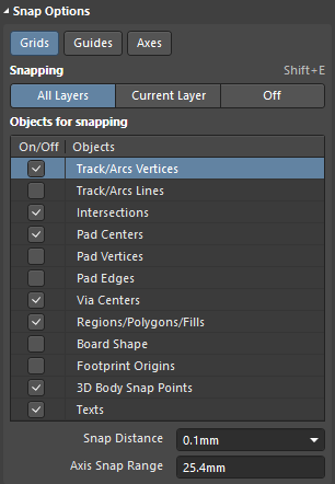
In the upper region, you can choose one or more types of grid objects to be snapped to: Grids, Guides or Axes. Grids is used to toggle whether the cursor will snap to the active workspace grid. When this option is enabled, the cursor will pull, or snap, to the nearest snap grid location. The active snap grid is displayed on the Status Bar at the bottom left of the workspace.

Guides is used to toggle whether the cursor will snap to manually placed linear or point snap guides. A Snap Guide will override the Snap Grid. Axes is used to toggle whether the cursor will axially-align (in either the X or Y direction) to the enabled Objects for snapping.
The Snapping region allows you to select the applicability of objects snapping.
- All Layers allows snapping on all available visible layers.
- Current Layer allows snapping only on the active layer.
- Off turns off snapping for all layers.
The Objects for snapping region allows you to choose the types of PCB objects to which the snap will be applied.
Snap Distance specifies the distance at which the snapping will be applied.
Axis Snap Range defines the distance within which X or Y axial-alignment will occur.