Creating Component Footprints
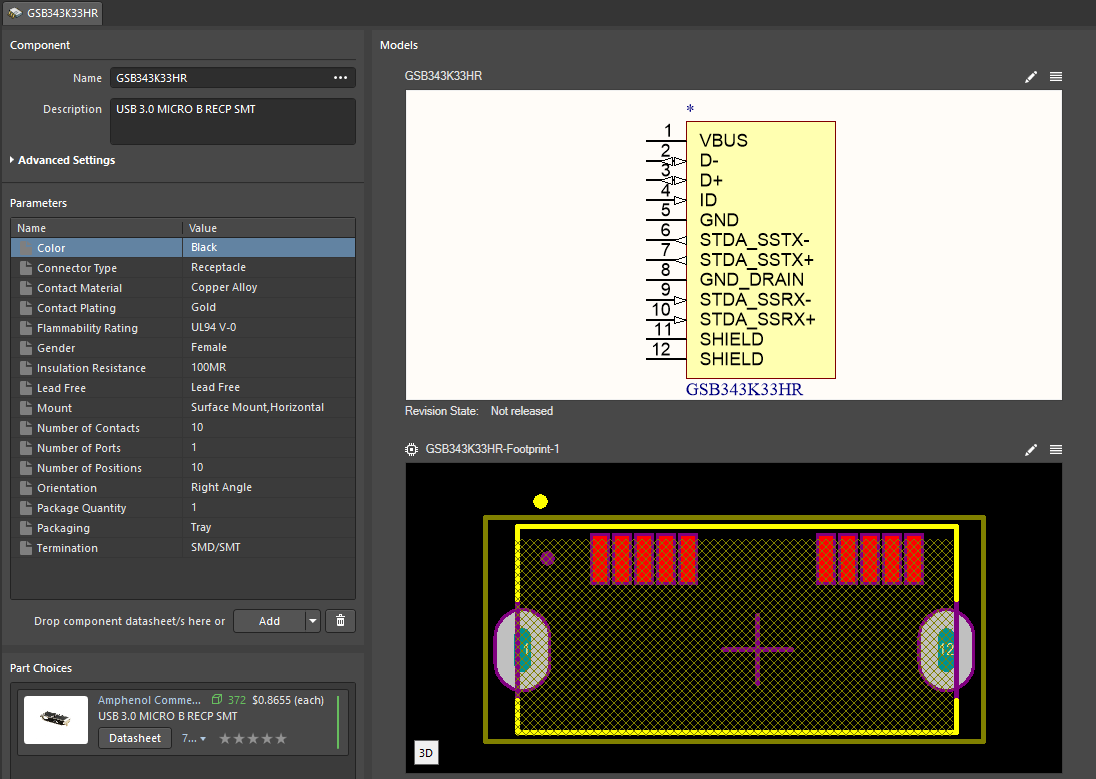
The next step in creating the component is to design the footprint. Component footprints contain a set of graphical primitives and copper pads or holes that will be connected to the conductors and will provide a metal connection. Also, the component itself will be soldered on these contact points, so their configuration should be fully consistent with the actual metal objects of the component. Any error in the placement of the footprint pads can lead to problems, up to and including the inability to assemble the final device, so library designers should be very careful when creating footprints. In Altium Designer, the process of creating footprints is as simple and convenient as possible while ensuring protection from errors as much as possible. With the help of the IPC Compliant Footprint Wizard, you can create any IPC components in just a few clicks by entering their parameters from the datasheet. Let’s create footprints for components GSB343K33HR and MBT3904DW1T1G, for which symbols were created in the last chapter. If you have closed the tabs with components, open them from the Projects panel.
Footprint Creation Using the IPC Compliant Footprint Wizard
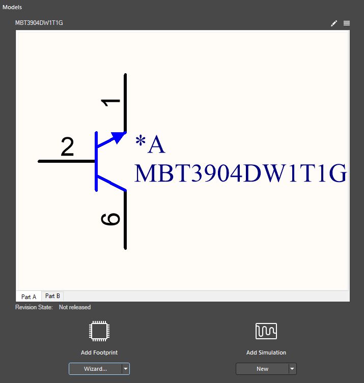
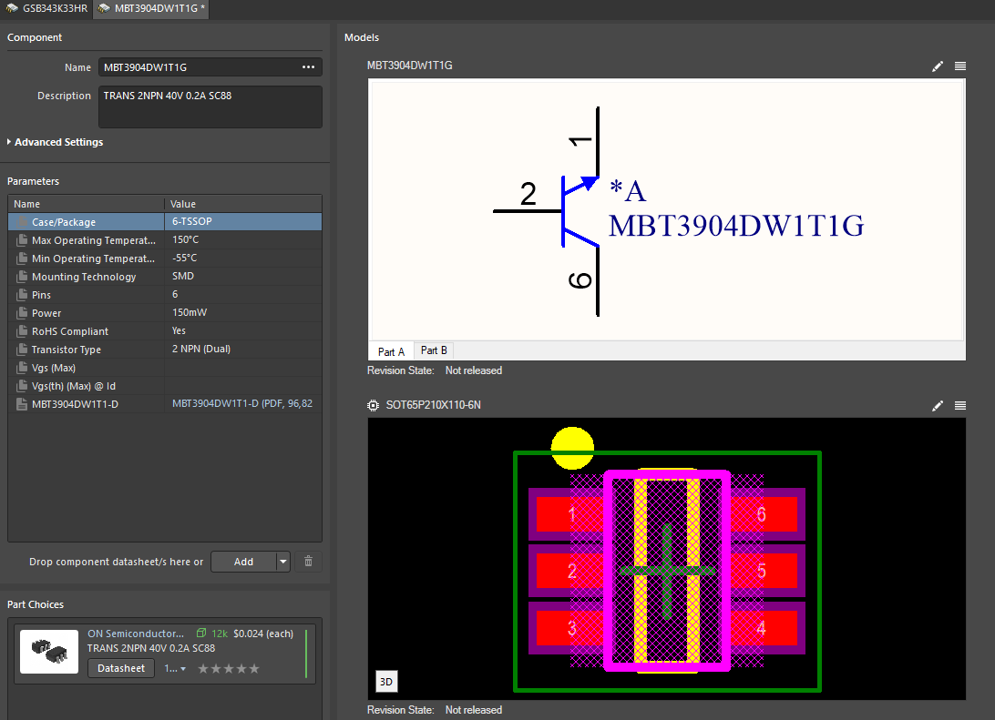
Activate the tab with the MBT3904DW1T1G component. This component is a standard IPC, so it can be created in a few clicks using the IPC Compliant Footprint Wizard. Click the Wizard button below the Add Footprint icon in the Models region of the component editor to start creating a new symbol.
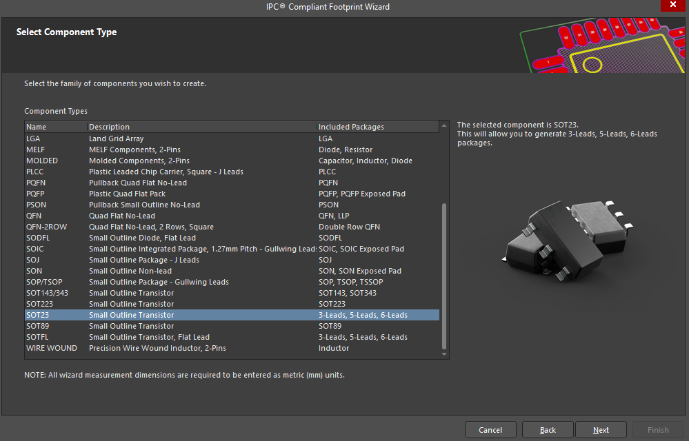
Click Next in the IPC Compliant Footprint Wizard. Select SOT23 in the Component Types list then press Next.
Select SOT23 6-Lead from the Package Type drop-down menu. Set all values using the component datasheet. Enable the Generate STEP Model Preview option in the lower-left corner to automatically create a 3D model of the generated component. Click Next after you have entered all the values.
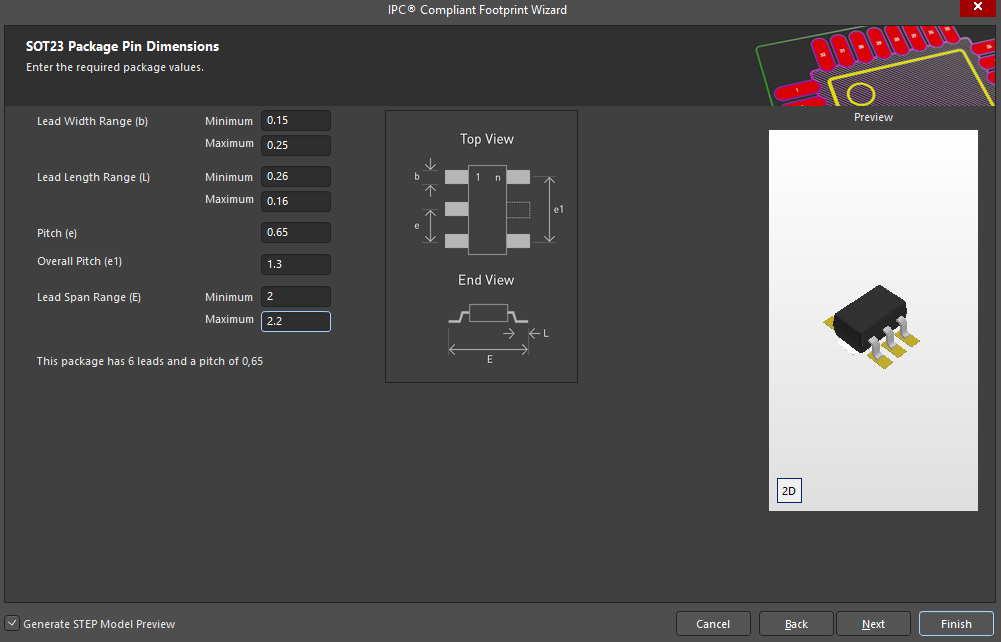
Enter all the required values on the SOT23 Package Pin Dimensions page using the information from the datasheet. Click Next after you have entered all the values.

Click the Next button twice since there is no need to change the calculated values for heel spacing or the default value for Round Off Pitch.
Select Level B - Medium density in the Board density Level drop-down menu. Click Next.
Click the Next button four times since there is no need to change the calculated or default values on those pages.
Define the Silkscreen Line Width value as 0.15 mm. Click Next without making any other changes until the IPC Compliant Footprint Wizard is complete page appears. Click Finish. After closing the Wizard, a generated footprint will open in a new tab of the design space. The generated footprint has all the necessary parameters, graphic designation, and assigned 3D models. Easy and incredibly quick, isn’t it?
Close the footprint tab. In the Component editor window, a footprint corresponding to the component appears in the Models region.
Now the component is fully ready to be released to the server. Select File > Save to Server from the main menus. Enter First component release in the Release Notes field then press OK. After a successful release, the MBT3904DW1T1G tab with the component will be closed and will appear in the server and is now ready for interaction for all workspace users.
Manual Footprint Creation
Open the GSB343K33HR tab. This connector cannot be created using the Wizard, so it must be created manually using the recommended PCB layout view from the datasheet. Click the arrow to the right of the Wizard button below Add Footprint then select New to create a new footprint.
In the Other region of the Properties panel in Library Options mode, change the units to mm.
According to the drawing, the pins are 1.35x0.4mm in size and their numbering is arranged in order starting from the left. All component pads (SMD, TH, Mixed) can be placed in the workspace. In the PcbDoc, select Place > Pad from the main menus. Press the Tab key. Define the following values in the Properties panel:
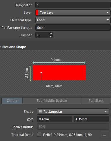
Designator: 1
Layer: Top Layer
Shape: Rectangular
(X/Y): 0.4mm/1.35mm
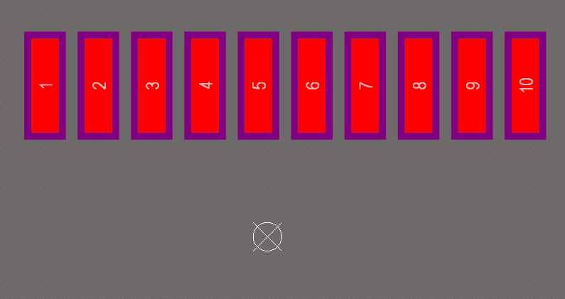
After all values have been specified, place the pad to the right and above the origin of the coordinates. The exact coordinates for all pads will be specified later.
After you have placed the first pad, the same pad is attached to the cursor and ready for placement, but with an increased Designator value of 2 by using automatic numbering of the pads. Place 9 more pads to bring the total in the working area to 10 pads.
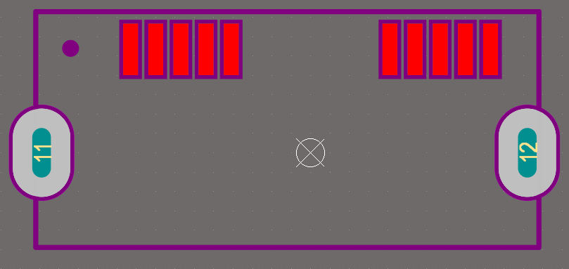
We now need to place two slot holes on the left and right side of the component. Select Place > Pad from the main menus. Press the Tab key. Define the following values in the Properties panel:
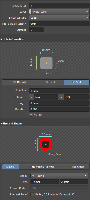
Designator: 11
Layer: Multi-Layer
Shape: Round
(X/Y): 1.5mm / 2.3mm
Hole Shape: Slot
Hole Size: 1.3mm
Length: 0.5mm
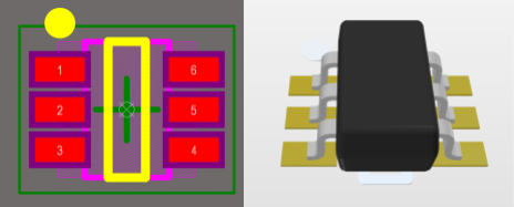
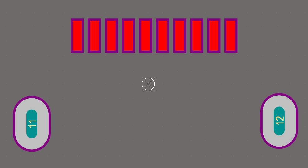
After all values have been specified, place one pad on the left and one pad on the right as shown in Figure 13.
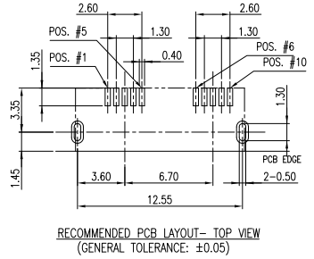
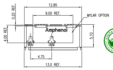
We now need to adjust the coordinates of all pads so that they correspond to the requirements of the drawing. The drawing with the recommended PCB layout shows that the dimensional anchorages are made from the slot holes and the distance between these holes is 12.55 mm, however, they are offset relative to the center.
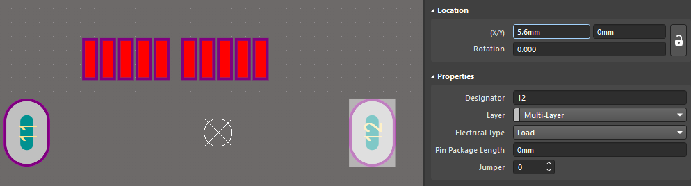
Select pad 11. Enter -(6.7/2+3.6) into the X coordinate field and 0 into the Y coordinate field. After entering, the pad will move to the desired coordinates.
Select pad 12. Enter -6,95+12,55 into the X coordinate field and 0 into the Y coordinate field.
Now let’s finish the SMD pads placement. They must be placed above the center and should have the same Y coordinate, therefore, we will calculate the Y coordinate first. Select all SMD pads and define their Y coordinate as 3.35-(1.35/2) . Divide that by 2 because the size binding goes to the upper edge of the contact area.
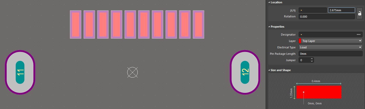
The next step is to set the correct X coordinate distance between the SMD pins. The drawing shows a 6.7 mm distance between the centers of pin 3 and pin 8. Therefore, pin 3 will be placed at -(6.7/2)=-3.35mm for the X coordinate and pin 8 at 3.35mm for the X coordinate because they are symmetrical. Let's calculate the pin 1 coordinates. The pitch between SMD pins in one group is equal to 0.65mm (2.6mm/4). Consequently, the edge pins will have an X coordinate equal to (3.35mm +0.65mm +0.65mm)=±4.65mm.
Select pin 1. Define its X coordinate as -4.65mm.
Define the X coordinate for pin 2 as -4mm.
Define the X coordinate for pin 3 as -3.35mm.
Define the X coordinate for pin 4 as -2.7mm.
Define the X coordinate for pin 5 as -2.05mm.

In Altium Designer, it is possible to automatically place selected pins evenly, but for this design, it is necessary to know the coordinates of the edge pins. Select pin 6. Since it should be placed symmetrically with pin 5, it has the same X coordinate, but with the opposite sign. Set the X coordinate for pin 6 as 2.05mm.
Select pin 10 and define its X coordinate as 4.65mm.
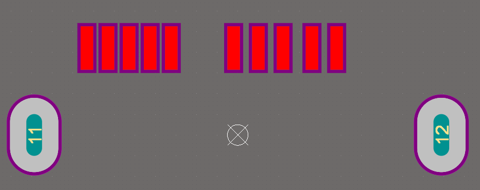
In order to perform this step correctly, all the remaining pins must be placed between pin 6 and pin 10! Select the right half of the pins, right-click on one of the selected pins then select Align > Distribute Horizontally. Now all pins of this group are evenly distributed between pins 6 and 10 and have pitch set to 0.65mm.
The main part of the component is ready. Now we need to add the graphics, which will be imported to the Assembly, Overlay, Courtyard, Designator, and Component Center layers. The graphics layer for the Assembly layer should include all component boundaries, including information on the first output.
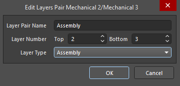
Open the View Configuration panel. Right-click on any layer in the Layers region then select Add Component Layer Pair. Select Assembly from the Layer Type drop-down menu. Click OK to add a new layer pair.
Make the Top Assembly layer active. This layer is required to place a drawing that will be necessary while designing the assembly drawing.
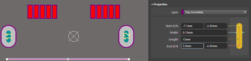
On this layer, we need to place a primitives set with the overall dimensions of the component and mark the first pin. Select Place> Line from the main menus. Draw a straight line below the central axis. After the line is placed, select it to define the following parameters in the Properties panel:
Start (X/Y): -7.1mm/-2.45mm
Width: 0.15mm
Length: 13mm
End (X/Y): 5.9mm/-2.45mm
The placed line should look like the figure below.
Add one more line to the Top Assembly layer with the following parameters:
Start (X/Y): -7.1mm/-2.45mm
Width: 0.15mm
Length: 6.1mm
End (X/Y): -7.1mm/3.65mm
The placed line should look like the figure below.
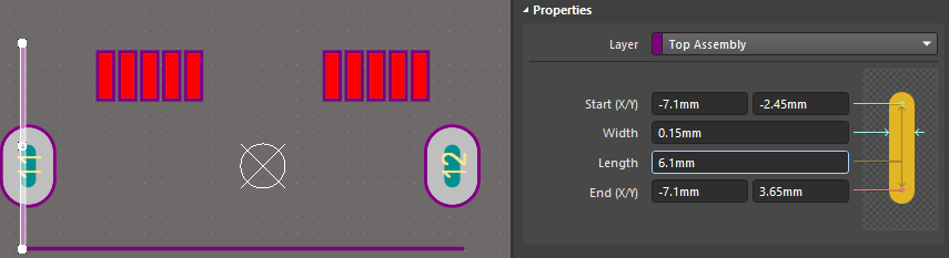
Copy and paste the placed lines one by one to finish the rectangle.
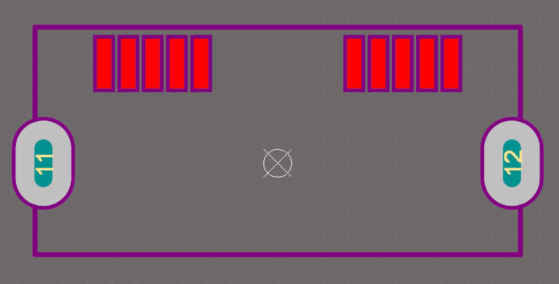
The next step is to add the indicator of the first pin. As a rule, it is indicated by a small circle placed inside the component contour. Select Place > Full Circle from the main menus and draw a little circle near the first pin of the component.
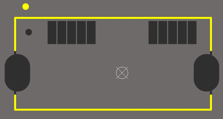
After adding the graphics for the assembly drawing, we need to add a graphic on the overlay layer (silkscreen). Graphics from this layer are used to simplify installation and subsequent repair of the device, and will also be drawn directly on the board. In most cases (except for BGA components), the silkscreen corresponds to the contour of the component but has a gap (~0.2-0.3mm) from all copper contact pads to avoid silkscreen ink getting on copper pads. In the case of the GSB343K33HR component, the gap between the top pins and the component contour is 0.25mm, so overlay lines can be drawn similar to the assembly drawing graphics added in the previous steps.
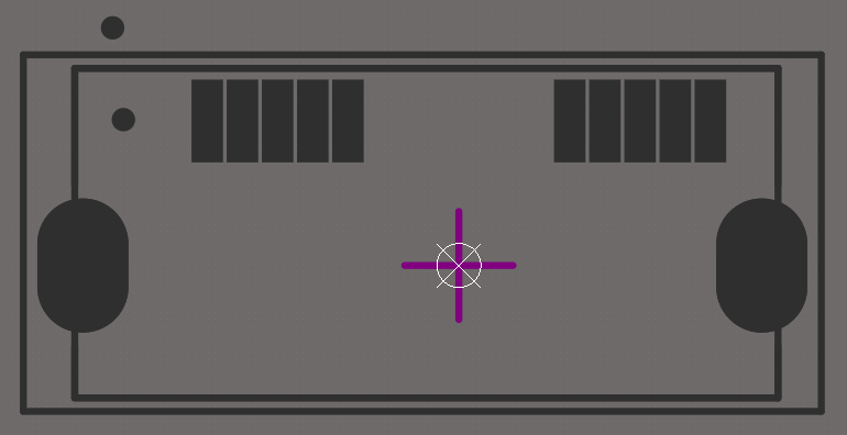
Make the Top Overlay layer active. Enable dimming in single layer mode by pressing Shift+S. Select Place > Line from the main menus. Press the Tab key then define the Line Width as 0.15mm in the Properties panel. Repeat lines for the contour of the component that is drawn on the Top Assembly layer. Do not forget that the copper plate of the slot holes (Pins 11 and 12) should also have a gap between the metal and silkscreen lines. Draw the first pin mark outside the component contour using Place > Full Circle. The final result of this step is shown in the figure below.
The next step is to create a Courtyard layer, which is necessary to implement component creation to a certain level of board placement density. This layer is represented by a rectangle with some gap either from the edge pins or from the component edge, whichever is larger. According to IPC-7531, there are three levels of mounting density:
- Level A (low mounting density, gap between pins/component edge = 0.5 mm)
- Level B (medium mounting density, gap = 0.25 mm)
- Level C (high mounting density, gap = 0.1 mm).
We need board density level B.
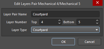
Open the View Configuration panel. Right-click on any layer in the Layers region then select Add Component Layer Pair. Select Courtyard from the Layer Type drop-down menu. Click OK to add a new layer pair.
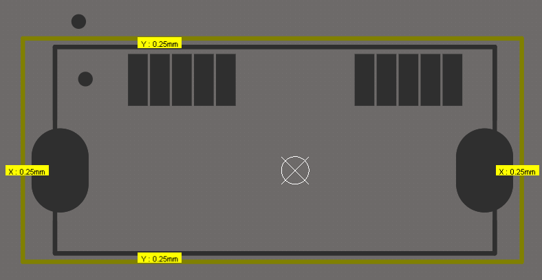
In order to realize the medium density of component placement, a rectangle with a gap of 0.25mm must be drawn from the edge pins and/or the edge of the component. With the current component, the gap must be provided from both the component contour (top and bottom edges) and the slot holes to the sides (as they are outside the component contour).
Make the Top Courtyard layer active. Using Place > Line, draw a rectangle with 0.15mm Line Width as shown in the figure below. You can check the resulting gap with the measuring tool by using Ctrl+M. The measuring should be performed between the centers of the Courtyard line and the Assembly line or edge of the slot hole. You can clear the measurement results using Shift+C.
Let’s add a Component Center layer for component center designations.
Open the View Configuration panel. Right-click on any layer in the Layers region then select Add Component Layer Pair. Select Component Center in the Layer Type drop-down menu. Click OK to add a new layer pair. The All Layers region should look like the figure below.
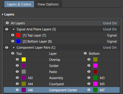
Make the Top Component Center layer active. Using Place > Line, draw a crosshair of lines in the center of the component.
The next step is to add the 3D model to the footprint. It is possible to connect a 3D model in .step, PARASOLID, or .sldprt format to the component. It is strongly recommended to add a 3D model for each component. This will offer more precise height rule matching, more pleasant PCB visualization, and a more accurate view while designing the assembly drawing in Draftsman. Let’s connect a 3D model to the footprint.
Download the .step model from here and place it in an appropriate location.
Open the View Configuration panel. Right-click on any layer in the Layers region then select Add Component Layer Pair. Select 3D Body from the Layer Type drop-down menu. Click OK to add a new layer pair. Make the Top 3D Body layer active.
Select Place > 3D Body from the main menus then select the downloaded .step model. Place the 3D model onto the workspace then select it. In the Properties panel, set the (X/Y) coordinates as -3.35mm and -1.9mm and define the Standoff Height as 1.2mm. Press the 3 key in the workspace to switch to 3D mode to verify the correct placement of the model. Save the footprint by pressing Shift+S and close the GSB343K33HR tab.
In the component editor, a footprint corresponding to the component appears in the Models region. Select File > Release to server from the main menus. Enter First component release in the Release Notes field then click OK. After a successful release, the GSB343K33HR tab will close and it will appear in the server and be ready for interaction for all workspace users.