Accessing the Layer Stackup
You can access the PCB Layer Stackup in the Altium web interface. There are three ways to work with the Layer Stackup associated with your project:
- Work in Progress Design,
- Releases, and
- Manufacturing.
The feature is available through Altium web interface.
Through the Info Icon ![]() . You can find general information about the board by clicking the info icon in the top-right corner:
. You can find general information about the board by clicking the info icon in the top-right corner:
Open a project in the Altium workspace.
Select Design > Name_of_the_Project.PcbDoc on the Project Pane, which appears on the left side of the editor (or click on ‘PCB’ in the top bar above the design).
Click the Info Icon ![]() in the top-right corner (it looks like a lowercase letter inside a circle).
in the top-right corner (it looks like a lowercase letter inside a circle).
Click Board Info. The dialog box will display the Board Size, Layers, Components, and Nets. Click Stackup View; the text will be highlighted in blue.

Through the Layers Panel. You can adjust all of the PCB layer-related information by clicking on this ![]() Layers icon.
Layers icon.
Open a project in Altium web workspace.
In the top-left corner of the editor, hover the mouse over the icon (Layers) . You will also see two sets of numbers separated by a slash (/). Click on it.
The first number of the set represents the number of visible layers, and the second number represents the total number of layers. To change the visibility of a layer, click over the layer once. An eye hide icon will appear in gray; this means the layer is not visible. 🎬 Toggle Visibility of Layers and Objects
Click Stackup View; it will be highlighted in blue.

Both methods of access will redirect to the same page:

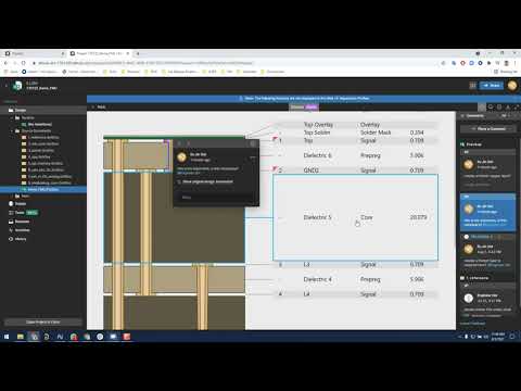
When nothing is selected, stackup properties will be on the right showing the Stackup Attributes. If you select a layer, a box with that layer's properties will be displayed on the right side of the window.

The thickness measurement (Thk) is displayed using the unit you chose when you saved the PCB doc. To switch to and from imperial (mil) or metric (mm), click the Back button in the upper-left corner.

If “Board Info” is displayed in the upper right-hand corner of the computer screen, click on it. Otherwise, click the Info Icon at the top-right corner and change units.

Return to the stackup viewer and ensure that the measurements are in the selected mil/mm setting.
Tip: You can place a comment on a layer or via. You can also mention users. To place a comment, click the icon in the top-right corner. You can find the details on how to comment in your design here.

Please note that viewing and commenting on Layer Stackup is only possible in the Altium Web Interface.