


Nets, ERC, connections
Physical and Logical Connectivity
On the schematic, you can create that connectivity by drawing a wire from one component to another - this is referred to as physical connectivity.
You can also connect one pin to another by placing a short Wire and a Net Label on each component pin. The software identifies these two net sections and connects them to form a single net. This type of connectivity is referred to as logical connectivity.
Physical connectivity allows a user to follow each wire as they study the circuit, but a lot of wires can result in a dense and busy schematic. On the other hand, Net Labels reduce the amount of wiring, but the user must scan the sheet to find all potential connections. As the designer, you are free to decide which connectivity model best suits your design, including a mixture of both techniques.

Place wires to create physical connectivity or use net labels to create logical connectivity.
Net Labels
Electrical connectivity between schematic component pins can be created by placing a wire between those pins. This is called physical connectivity since the pins are physically connected with a wire. Connectivity also can be created logically by using suitable net identifiers, such as net labels. As well as providing a human-friendly identifier for a net, a net label allows you to connect points on a circuit without actually physically wiring them together.
Availability
Net labels are available for placement in the Schematic Editor only in the following ways:
-
Choose Place » Net Label from the main menus.
-
Click the Net Label button (
 ) in the graphic objects drop-down on the Active Bar located at the top of the design space. (Click and hold an Active Bar button to access other related commands. Once a command has been used, it will become the top-most item on that section of the Active Bar.)
 -
Right-click in the design space then choose Place » Net Label from the context menu.
-
Click the
button on the Wiring toolbar.
Placement
After launching the command, the cursor will change to a cross-hair and you will enter net label placement mode with a net label floating on the cursor:
-
Press Tab to open the Net Label mode of the Properties panel with the Net Name field selected and ready for editing; enter the new net name.
-
Position the net label so that its bottom-left corner touches the object to which you want to assign it then click or press Enter to place the net label.
-
Continue placing further net labels, or right-click or press Esc to exit placement mode.
Additional actions that can be performed during placement while the net label is still floating on the cursor and before the center point of the net label is anchored are:
- Press the Tab key to pause the placement and access the Net Label mode of the Properties panel in which its properties can be changed on the fly. Click the design space pause button overlay (
 ) to resume placement.
 - Press the X or Y keys to flip the net label along the X-axis or Y-axis.
- Press the Spacebar to rotate the net label counterclockwise or Shift+Spacebar for clockwise rotation. Rotation is in increments of 90°.
Considerations during placement:
- The electrical hotspot on a net label is the lower left corner, therefore, this corner must touch the wire, bus, or signal harness for a valid connection to be made.
- If the Net property of the net label is entered before it is placed and the value entered has a numeric ending, each subsequent net label will auto-increment this numeric value. This behavior is configured in the Auto-Increment During Placement options on the Schematic – General page of the Preferences dialog. For net labels, only the Primary field applies; the Secondary field applies when the object has multiple fields, such as a Pin.
Graphical Editing
The net label can be edited graphically using what is known as in-place editing. To edit a net label string in place, click once to select, pause then click a second time to enter edit mode.
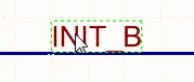 |
Click once to select the string. |
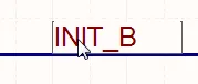 |
Pause, then click a second time to enter in-place edit mode. |
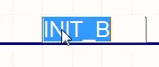 |
The string has been selected, ready to type in a replacement string. |
Once editing is complete, press Enter or click away from the string to exit in-place editing mode.
ERC
To validate your design, choose the Validate PCB Project <ProjectName> command from the main Project menu. To validate the project focused in the Projects panel, you can also use the Validate Project command from the right-click menu of the project's entry or the  control at the top of the panel.

Validate your design using the Validate PCB Project <ProjectName> command.
The software checks for logical, electrical, and drafting errors between the Unified Data Model and project checking settings. If validation errors and warnings are enabled for display on the schematic (enabled on the Schematic – Compiler page of the Preferences dialog), an offending object will display a colored squiggle beneath it. Hovering over the object will display a pop-up hint that summarizes the violation. A notification is also displayed in the Messages panel.
Resolving a Warning or Error
It is important to address each warning or error that is detected. The default error settings tend to be conservative since it is better for the software to err on the side of being cautious and let you decide if the testing boundaries can be relaxed. For example, your design may require IO pins to be connected to Input ports, requiring you to adjust the appropriate cell in the Connection Matrix tab. Another common error check to be changed is the Nets with no driving source, requiring you to disable that check in the Error Reporting tab.
There will be situations when you want to test the entire design for a certain condition, but you want to ignore a warning/error at a specific point in the circuit. For example, you might want to allow a net to be renamed at a specific location, but only in that location. This can be done by placing a No ERC directive at that location.
