Welcome, Guest

Sign in to learn, create, and do more with the product you love.

News & Updates

Filters:
Tag
Blog
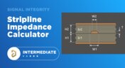
Stripline Impedance Calculator

Striplines provide some advantages over microstrips as they take advantage of natural shielding and coupling from nearby ground plane layers. Although they tend to experience higher losses due to total confinement in the dielectric, they can be thinner due to the high dielectric constant used in internal layers of a PCB. Use our free impedence calculator to help you determine the correct width needed to hit a target impedance.

Embedded thumbnail for Query Language: What is It For?
How-To's
Query Language: What is It For?

A PCB project contains many different objects. How to manage them? How to find the right ones quickly and efficiently? This video starts the series about query language. Learn the language commands and how to use them and expand your possibilities!

Blog
Which Types of Opto-Isolators Are Right For Your Signal?

An optoisolator is a cool electronic device that can be used to pass information between a diode without passing an electrical current. There are many great applications for these, but do you know which one is right for you?
Blog
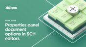
Properties panel document options in SCH editors

The Properties panel provides access to the properties of documents and objects. The contents of the panel change depending on the active document or the selected object. This blog will quickly go over some of need to know options around the properties panel in the schematic document.

Embedded thumbnail for PCB design with BGA: Via-in-Pad
How-To's
PCB design with BGA: Via-in-Pad

We’ll teach you how to use Via-in-pad to reduce inductance, improve signal integrity, and improve power distribution system performance.

Embedded thumbnail for Design RF PCB: Distributed-Element Circuits
How-To's
Design RF PCB: Distributed-Element Circuits

Distributed-element circuits are a topology of a particular shape and size. Filters, power dividers, directional couplers can be built from them. Being calculated in third-party CAD, the topology of such elements can be easily imported into Altium Designer, and we will show you how to do it!

Embedded thumbnail for How to work with components on a rigid-flex board in MCAD
How-To's
How to work with components on a rigid-flex board in MCAD

With MCAD Codesigner you can quickly add and move components from your MCAD tool and update the design automatically in Altium Designer. We’ll show you how to. Add a new component, move components, and change a component’s region in MCAD, and update it to your design in Altium Designer.

Embedded thumbnail for LSM: Impedance profile
How-To's
LSM: Impedance profile

Creating Impedance profiles for transmission lines and how to apply them to the board

High-Speed PCB Stackup Design
Blog
The High-Speed PCB Stackup Design Challenge

Even with all the good guidelines out there for high speed design, there are particular aspects of stackup construction and their relation to building boards that get overlooked. This blog is goes beyond just the typical SI/PI guidelines and looks at these problems from more of an engineering perspective.

Embedded thumbnail for Multichannel Schematic: Creating Channels
How-To's
Multichannel Schematic: Creating Channels

Altium Designer makes creating single and multichannel designs effective and quick. We’ll show you how to create and annotate output and input channels in your design.

Embedded thumbnail for How to efficiently use Blankets?
How-To's
How to efficiently use Blankets?

Blanket is a powerful tool for group assignment of properties in schematic documents. It makes it easier and faster to assign circuit classes, differential pairs, and design rules within schematic documents. This video provides instructions on how to use blanket to simplify work in your designs.

stitching vias
Blog
Everything You Need to Know About Stitching Vias

Stitching vias are something you often see spread around the surface layer of a PCB, but what are they? and should you be using them? In this guide, we'll go over some of the standard uses of stitching vias and when they should be used in a PCB.

Embedded thumbnail for High Speed: XSignals for DDR3/DDR4
How-To's
High Speed: XSignals for DDR3/DDR4

In high speed design DDR3 and DDR4 memory chips can utilize xSignal classes to match track lengths from the controller to the memory chip easily and quickly. We’ll show you how using the xSignals wizard.

Embedded thumbnail for Design RF PCB: routing (any angle, arc)
How-To's
Design RF PCB: routing (any angle, arc)

It is worth taking a responsible approach to the shape and size of the RF signal conductors. In this video we will cover some practical aspects of working with routing such nets in Altium Designer.

PCB Stackup Basics
Blog
PCB Stackup Basics

In comparison to the build-up of a PCB, the stackup is more concerned with the electrical type of each layer, that is are we working with signals, power, or ground. Continue reading to learn how you can optimize your layer stack.

Embedded thumbnail for Draftsman Document: Snapping
How-To's
Draftsman Document: Snapping

Snapping using the grids and snapping tools in Altium Designer’s Draftsman Editor gives you a lot of control over how you create and annotate primitives and components. We’ll show you how easy it is to use snapping in the Drafstman Editor.

Embedded thumbnail for High Speed: XSignals
How-To's
High Speed: XSignals

You can create, configure, and utilize xSignals in Altium Designer to make your design process more efficient and effective. We’ll show you how to do it manually, using the more comprehensive Create xSignals command, and using the xSignal wizard.

Embedded thumbnail for DFM and fab cost/time constraints: What is annular ring and how to configure it
How-To's
DFM and fab cost/time constraints: What is annular ring and how to configure it

The minimum dimension from the wall of the aperture to the edge of the pad is called an annular ring, and we can configure it with Altium Designer. We’ll show you how to get started and manage the annular ring in your design rules.

Embedded thumbnail for Altium 365 Getting Started: Gerber Compare
How-To's
Altium 365 Getting Started: Gerber Compare

The task of comparing different versions of manufacturing files usually arises when the electrical engineer needs to check and confirm the manufacturer's edits or clarify details of changes before starting production. In Altium 365 you can perform an automatic comparison of Gerber files.

Tag
Article preview
Blog
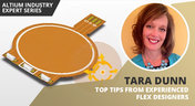
Top Tips from Experienced Flex Designers

This article describes the best hints and tips for designers of rigid-flex circuits. These tips include choosing the most appropriate material, suggestions for coordinating the PCB with the manufacturer, and a set of rules to be followed while PCB design. 

Article preview
Blog
How Do Capacitor Mounting Structures And Footprints Impact Total Inductance?

There are a number of factors at play when it comes to the impact of inductance on high-frequency power distribution systems. This article will focus on the inductance of the capacitor footprint along with the inductance of vias from the capacitor footprint to the PCB power planes. Included are the various types and sizes of footprints for ceramic capacitors as well as a footprint for a tantalum capacitor; how changing the footprint impacts inductance and test results obtained for different capacitors.


Article preview
Blog
How to Perform Differential Pair Tuning in Altium Designer 20

In order to properly suppress common-mode noise, differential pairs must be routed in parallel, with perfect symmetry, and with matched lengths. In real PCBs, meeting these three objectives isn’t always possible. Instead of eyeing out your different pair lengths, the interactive routing tools in Altium Designer make differential pair length matching easy. You can encode permissible length mismatches as design rules as part of controlled impedance routing, or you can manually perform differential pair tuning using a variety of meandering styles. Here’s how this works in Altium Designer.

Blog
Driving Haptic Vibration and Feedback in Wearables

Augmented reality, virtual surgery, limb replacements, medical devices, and other new technologies need to incorporate haptic vibration motors and feedback to give the wearer a full sense of how they are interacting with their environment. Unless these cutting-edge applications include haptic vibration and feedback, users are forced to rely on their other four senses to understand the real or virtual environment.

Article preview
Blog
Back Drilling Example in Altium Designer: One of the Easiest Ways to Improve Signal Integrity

Over the last 20 years, electronic devices have become increasingly sophisticated. Less than two decades ago, just having a mobile phone to make calls was rare; today, our phones power our lives. To meet the growing demand for smartphone technology, technology has become faster, more functional, and intuitive. Improvements to the component base have streamlined processes while reducing manufacturing costs.

Article preview
Blog
Is it Simultaneous Switching Noise or Crosstalk?

Going deeper into crosstalk, there is always the issue of verifying EMI/EMC compliance through test and measurement. With the multitude of signal integrity problems that can arise in real PCBs, how can the astute designer distinguish them all? Some problems are clearer than others, with specific signal integrity measurements being developed for testing and measuring particular aspects of signal behavior. The fact is, multiple signal integrity problems could be present on a single interconnect simultaneously.

Article preview
Blog
Sharing PCB Data with Manufacturers in the Cloud

Once you’ve finished your new project and you’re ready to push it to your manufacturer, you’ll normally be stuck in an endless email chain with an engineer, or you’ll have to share cloud links with each other. The cloud sharing and design release tools in Altium Designer and Altium Concord Pro are a huge help in this area. In this post, I’m going to take an existing project I’ve worked with in a number of recent blogs, create some fabrication and assembly documentation, and finally push this data to a manufacturer using Altium Concord Pro.

Article preview
Blog
The Great PCB Layout "Rules of Thumb" Debate Rages On

To this day, I still see many PCB layout “rules of thumb” that first became common nearly 20 years ago. Do these rules still universally apply? The answer is a firm “maybe.” The discussion around PCB layout rules of thumb is not that these rules are correct or incorrect. The problem is that the discussion around these rules often lacks context, leading to the always/never type of discussion seen in some popular forums. My goal in this article is to communicate the context behind the common PCB design rules.

Article preview
Blog
How to Design Your PCB Test Coupon and What You Can Test

As the operating speed of components has increased, controlled impedance is becoming more common in digital, analog, and mixed-signal systems. If the controlled impedance value for an interconnect is incorrect, it can be very difficult to identify this problem during an in-circuit test. However, testing is normally performed on a PCB test coupon, which is manufactured on the same panel as the PCB. If you want to get through board spins quickly and aid future designs, you might consider designing a test coupon and keeping it handy for future designs.

Article preview
Blog
Altium DbLibs and Electronic Components in the Cloud with Altium Designer 20.1

Altium’s DbLib support is one of the oldest and most loved features of Altium Designer for managing electronic components and their data. They’ve been present in the software world since before I could fathom the existence of Ohm’s law. Altium 20.1’s new Component Sync feature allows you to synchronize virtually any database or database Library with Altium 365, taking advantage of both approaches strengths.

Article preview
Blog
What is a Schematic Netlist for Your PCB?

If you’ve created your next great schematic, there is a lot going on behind the scenes in your design software. A schematic netlist is one of the central pieces of information that will be used in multiple features in your design software to create a real PCB. Your schematic netlist provides both electrical connectivity information, and reflects the functional structure of your design data in a single set of data.

Article preview
Blog
How to Select an Inductor for a Buck Converter

An SMPS is one of those quiet (yet electrically noisy) devices that makes your favorite electronics run smoothly. Among the numerous DC-DC converter topologies, a buck converter finds plenty of uses for stepping down the input voltage to a lower level while providing high efficiency power conversion. A common question around component selection for these power converters is how to select an inductor for a buck converter. The goal in working with an inductor and other components in a buck converter is to limit power loss to heat and while minimizing current ripple.

Article preview
Blog
US Department of Transportation Seeking Alternatives to GPS

GPS-capable devices range from your phone to your smartwatch; simply type in your destination and follow the directions. Simple, right? According to the Washington Post, we should all stop using GPS as it’s ruining the navigation centers of our brains. Despite the neurological effects on perception and judgment, the U.S. Department of Transportation (DOT) aims to find alternatives to GPS to provide redundancy.

Article preview
Blog
Bluetooth 5.1 SoC vs. Module: Which is Best for Your Design?

The list of features available in Bluetooth just got a little longer since the release of Bluetooth 5.1. If you want to incorporate a Bluetooth 5.1 SoC into your new product, you have two primary options for bringing this component into your board. The first is as an SoC that mounts to your board just like any other component. The other option is to bring a module into your new board—directly onto the surface layer. Here’s what you need to know about a Bluetooth 5.1 SoC or module in your next IoT product.

Article preview
Blog
USB Power Delivery for Your Next Project

Since its introduction in the late 90s, the USB standard has never ceased to grow in popularity. There has been a growing trend toward USB being a power delivery interface with data, rather than a data interface that can supply power, as the 1.0 specification originally intended. To supply the increasing thirst for power over USB, the USB 3.0 Spec with Type-C began implementing the Power Delivery standard, which you should consider using for your next electronics project.

Tag
NEW
Embedded thumbnail for Connect Requirements Directly to Your PCB Design
New in Altium's Software
Connect Requirements Directly to Your PCB Design

See how the Requirements Portal integration in Altium Designer simplifies requirements management by bringing system requirements directly into your PCB design workflow. Connect requirements to design documents, assign tasks, track verification in real time, and keep your entire team aligned with seamless synchronization in Altium 365.

NEW
Embedded thumbnail for SFP Connector Routing: High-Speed Differential Pair Design Tips
How-To's
SFP Connector Routing: High-Speed Differential Pair Design Tips

Discover practical SFP and SFP+ routing tips in our latest video, inspired by a real question from the Altium subreddit. We cover how aggressive serpentine length tuning can be, how to reduce impedance discontinuities in tight meanders, and how meandering influences mode conversion at 10G and higher data rates.

Embedded thumbnail for Handle High-Density PCB Layouts with Ease
New in Altium's Software
Handle High-Density PCB Layouts with Ease

Push the limits of PCB design with support for up to 128 signal layers, empowering the development of even the most complex, high-density boards.

Embedded thumbnail for Skip Layer Routing for RF: Control Impedance & Cut Insertion Loss
How-To's
Skip Layer Routing for RF: Control Impedance & Cut Insertion Loss

Discover our latest video and learn how RF designers use a deeper ground plane to minimize skin-effect resistance, improve signal integrity over long high-frequency routes, and optimize impedance matching for oversized SMT pads in antenna launches and coaxial connectors.

Embedded thumbnail for Just Released: ODB++ Intellectual Property Protection
New in Altium's Software
Just Released: ODB++ Intellectual Property Protection

ODB++ Intellectual Property Protection lets you control exactly what design data is included in the ODB++ output, ensuring each manufacturing partner receives only the information needed for their specific fabrication or assembly tasks.

Embedded thumbnail for Future of Electronics Development in Security and Aerospace
How-To's
Future of Electronics Development in Security and Aerospace

See the highlights from Altium's executive event in Hamburg, where Security and Aerospace leaders explored AI-driven development, digital engineering, supply chain resilience, and the future of mission-critical electronics.

Embedded thumbnail for Create Clearance Rules Faster and with Less Effort
New in Altium's Software
Create Clearance Rules Faster and with Less Effort

Setting up clearance rules is now more intuitive in the Constraint Manager. Choose the Simple view for faster configuration with grouped object types, or the Advanced view when you need detailed, matrix-based clearance control.

Embedded thumbnail for Mastering HDI Design Rules in Altium Designer
How-To's
Mastering HDI Design Rules in Altium Designer

In our latest Altium Academy tutorial, we guide you through configuring the essential HDI PCB design rules in Altium's software. You'll learn how to use your manufacturer's fabrication capabilities to create accurate design rules and constraints for your PCB.

Embedded thumbnail for Search, Filter, and Navigate PCB Designs Faster
New in Altium's Software
Search, Filter, and Navigate PCB Designs Faster

The Web Viewer now features a redesigned search experience for faster access to PCB design data across supported CAD formats. A lightweight, intuitive interface lets you begin with simple search terms and progressively refine results using contextual suggestions.

Embedded thumbnail for Gain Better Control Over Wire Bond Visibility
New in Altium's Software
Gain Better Control Over Wire Bond Visibility

New bond wire visibility controls give you greater flexibility when working with wire-bonded boards and footprints, making it easier to focus on the details that matter most.

Embedded thumbnail for Coming Soon: Selectable Harness Source Within Multi-board Design
New in Altium's Software
Coming Soon: Selectable Harness Source Within Multi-board Design

Selectable Harness Source Within Multi-board Design enables harness projects to drive system connectivity while maintaining bidirectional synchronization between multi-board schematics and harness wiring diagrams for improved accuracy and easier design management.

Embedded thumbnail for Choose the Simbeor Version for Your PCB Calculations
New in Altium's Software
Choose the Simbeor Version for Your PCB Calculations

The PCB Editor now lets you choose the Simbeor version used for delay and impedance calculations, giving you more flexibility and consistency across your design workflows.

Embedded thumbnail for Improve PCB Editor Performance with Via Instancing
New in Altium's Software
Improve PCB Editor Performance with Via Instancing

The PCB Editor now uses via instancing to generate geometry for each via individually, providing greater flexibility and a more advanced approach to managing vias in PCB designs.

Embedded thumbnail for GSSG Stackup Deep Dive: Routing, Impedance, and HDI
How-To's
GSSG Stackup Deep Dive: Routing, Impedance, and HDI

A ground-signal-signal-ground (GSSG) stackup rethinks the traditional four-layer PCB structure by moving the ground planes to the outer layers and routing signals on the two inner layers. In this Altium Academy deep dive, we review a real one-minute design review submission and demonstrate how to configure a GSSG stackup properly using the Layer Stack Manager.

Embedded thumbnail for Generate IPC-7351B Compliant Footprints with More Control
New in Altium's Software
Generate IPC-7351B Compliant Footprints with More Control

The IPC Compliant Footprint Wizard has been updated to improve IPC-7351B compliance across supported package types. Enhancements include footprint calculations, package outlines, silkscreen and courtyard generation, layer mapping, density table behavior, and new pad trimming controls for gullwing packages, with support added to the batch generator Excel template.

Embedded thumbnail for Add Unit-Aware Temperature Coefficient Parameters
New in Altium's Software
Add Unit-Aware Temperature Coefficient Parameters

Component templates in a connected Workspace on the Altium Platform now include support for Temperature Coefficient (ppm/°C) as a unit-aware user parameter type. This makes it possible to define temperature coefficient values directly within the template using the appropriate units.

Tag
Your search returns no results.