Connect Requirements Directly to Your PCB Design
The Requirements Portal integration in Altium Designer enhances PCB design by connecting system requirements directly to the design environment. You can place requirements on schematics or PCB documents, assign tasks, and track verification status in real time, ensuring data synchronization within Altium 365.
Recommended Content:
- Visit the Requirements Portal page.
- Learn more about the Octopart Discover, Altium Develop, and Altium Agile platform solutions.

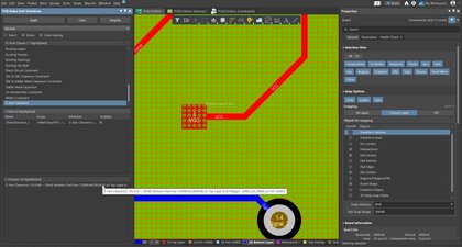
Handle High-Density PCB Layouts with Ease
You can now create up to 128 signal layers in your PCB design, enabling the creation of more complex and high-density boards.
Recommended Content:
- To learn more about PCB Layout in Altium Designer, visit the resource page.
- Visit the PCB Layout documentation page.
- Learn more about the Octopart Discover, Altium Develop, and Altium Agile platform solutions.

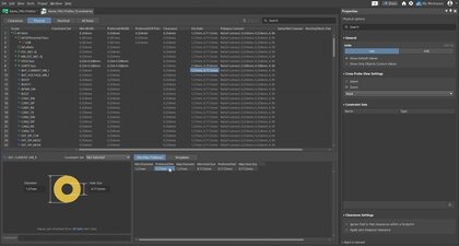
Create Clearance Rules Faster and with Less Effort
Clearance rule configuration in the Constraint Manager now includes Simple and Advanced views. The Simple view groups related object types to make rule setup easier, while the Advanced view provides a detailed clearance matrix for more precise control.
Recommended Content:
- To see an overview about the Constraint Manager, visit the feature page.
- Visit the Constraint Manager documentation page.
- Learn more about the Octopart Discover, Altium Develop, and Altium Agile platform solutions.

Altium Designer 26
Gain Better Control Over Wire Bond Visibility, Improve PCB Editor Performance with Via Instancing, Choose the Simbeor Version for Your PCB Calculations
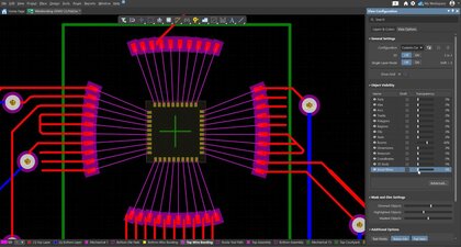
Gain Better Control Over Wire Bond Visibility
We've added new visibility controls for bond wires when working with boards or footprints that include wire bonding.
Recommended Content:
- To see an overview, visit the Wire Bonding feature page.
- Learn more about the Octopart Discover, Altium Develop, and Altium Agile platform solutions.
Improve PCB Editor Performance with Via Instancing
The PCB editor now builds the geometry for each via instance rather than relying on a via template, using an approach called via instancing.
Recommended Content:
- To learn more about PCB Layout in Altium Designer, visit the resource page.
- Visit the PCB Layout documentation page.
- Learn more about the Octopart Discover, Altium Develop, and Altium Agile platform solutions.
Choose the Simbeor Version for Your PCB Calculations
You can now control which version of Simbeor is used when calculating delay and impedance in the PCB editor.
Recommended Content:
- To learn more about PCB Layout in Altium Designer, visit the resource page.
- Visit the PCB Layout documentation page.
- Learn more about the Octopart Discover, Altium Develop, and Altium Agile platform solutions.
Generate IPC-7351B Compliant Footprints with More Control, Present Large Harness Tables More Clearly, Improve Readability with Custom Pin Spacing
Generate IPC-7351B Compliant Footprints with More Control
The IPC Compliant Footprint Wizard has been updated across supported existing package types to better align generated footprints with IPC-7351B. The update includes changes to footprint calculation, package outline, silkscreen, courtyard, layer mapping, and density table behavior. It also adds pad trimming control for gullwing packages, including support in the batch generator Excel template. Molded package inputs have been clarified with an added lead span range parameter and a renamed body length range parameter.
Recommended Content:
- Learn more about the Octopart Discover, Altium Develop, and Altium Agile platform solutions.

Present Large Harness Tables More Clearly
Harness Draftsman now supports splitting a connection table across multiple pages in a *.HarDwf document. A new page height limit lets you control how much of the table is shown on each page. This makes large harness connection tables easier to present in drawings without shrinking the table or moving the data to a separate document.
Recommended Content:
- To see an overview about the Harness Design tool, visit the feature page.
- Visit the Harness Design documentation page.
- Learn more about the Octopart Discover, Altium Develop, and Altium Agile platform solutions.

Improve Readability with Custom Pin Spacing
Component templates in a connected Workspace on the Altium Platform now support Temperature coefficient (ppm/°C) as a unit-aware user parameter data type. This allows temperature coefficient values to be defined with the correct units directly in the template.
Recommended Content:
- Learn more about the Octopart Discover, Altium Develop, and Altium Agile platform solutions.

Improve Your 3D Wire Bonding Workflow, Customize Your ODB++ Output for Each Partner, Improve Readability with Custom Pin Spacing
Improve Your 3D Wire Bonding Workflow
Wire bonding design now includes new 3D capabilities for defining bond wire shape, checking clearances, supporting import/export workflows, and managing wire bonding objects.
Recommended Content:
- To see an overview, visit the feature page.
- Learn more about the Octopart Discover, Altium Develop, and Altium Agile platform solutions.

Customize Your ODB++ Output for Each Partner
You can now control exactly what design information is included in ODB++ output for different manufacturing recipients. This includes selecting signal layers for export, choosing whether the netlist is included, disabled, or neutralized, and controlling whether component data is removed or exported without properties.
Recommended Content:
- Visit the fabrication outputs documentation page.
- Learn more about the Octopart Discover, Altium Develop, and Altium Agile platform solutions.

Improve Readability with Custom Pin Spacing
You can now define a custom vertical margin for a pin’s designator and name. This can be configured globally through Schematic Preferences or locally within individual Pin properties.
Recommended Content:
- To learn more about Schematic Capture in Altium Designer, visit the resource page.
- Visit the Schematic Capture documentation page.
- Learn more about the Octopart Discover, Altium Develop, and Altium Agile platform solutions.

Create IPC-Aligned Footprints with Less Effort, Make Via Rule Configuration More Intuitive, Detect Z-Axis Clearance Issues Earlier
Create IPC-Aligned Footprints with Less Effort
The default values for the Solder Mask Expansion rule in PCB documents and rule-driven solder mask expansion in PCB library documents are now set to 0 mil instead of 4 mil.
Recommended Content:
- To learn more about PCB Layout in Altium Designer, visit the resource page.
- Visit the PCB Layout documentation page.
- Learn more about the Octopart Discover, Altium Develop, and Altium Agile platform solutions.
Make Via Rule Configuration More Intuitive
When defining a routing via style rule in the physical view, you can now specify minimum, maximum, and preferred values for both diameter and hole size. Also, new controls allow you to quickly switch between Min/Max/Preferred constraints and template-based definitions.
Recommended Content:
- To see an overview about the Constraint Manager, visit the feature page.
- Visit the Constraint Manager documentation page.
- Learn more about the Octopart Discover, Altium Develop, and Altium Agile platform solutions.
Detect Z-Axis Clearance Issues Earlier
The Z-axis clearance rule allows you to check the shortest distance between copper across layers by defining clearances between specific net classes, differential pairs, or even by applying schematic parameter directives.
Recommended Content:
- To learn more about PCB Layout in Altium Designer, visit the resource page.
- Visit the PCB Layout documentation page.
- Learn more about the Octopart Discover, Altium Develop, and Altium Agile platform solutions.
Import and Export with Modern Mechanical Models, Clearly Show Jumper Wires in Your Harness Designs, Keep Your Harness Designs in Sync with Library Updates
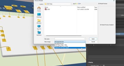
Import and Export with Modern Mechanical Models
We've added support for SOLIDWORKS 2024 and 2025 part models for importing 3D bodies and updated the Parasolid export to version 35.1.
Recommended Content:
- To learn more about PCB Layout in Altium Designer, visit the resource page.
- Visit the PCB Layout documentation page.
- Learn more about the Octopart Discover, Altium Develop, and Altium Agile platform solutions.
Clearly Show Jumper Wires in Your Harness Designs
Jumper wires that connect two cavities within the same connector are now correctly represented in Layout Drawings.
Recommended Content:
- To see an overview about the Harness Design tool, visit the feature page.
- Visit the Harness Design documentation page.
- Learn more about the Octopart Discover, Altium Develop, and Altium Agile platform solutions.
Keep Your Harness Designs in Sync with Library Updates
The "Update From Libraries" feature is expanded to support more harness-related objects in Wiring Diagrams and Layout Drawings.
Recommended Content:
- To see an overview about the Harness Design tool, visit the feature page.
- Visit the Harness Design documentation page.
- Learn more about the Octopart Discover, Altium Develop, and Altium Agile platform solutions.
Clearly Communicate Your True Harness Length, Save Time Looking at Differences in BOM CoDesign, Protect Component Lifecycle States During Synchronization
Clearly Communicate Your True Harness Length
The harness bundle length is now automatically set to match the drawn length in the layout, and when you enter the real physical length and it is different, Altium Designer clearly marks the bundle with a 'Not to Scale' break symbol. Also, when a covering extends over a bundle with a break symbol, a corresponding break symbol will be displayed for that covering.
Recommended Content:
- To see an overview about the Harness Design tool, visit the feature page.
- Visit the Harness Design documentation page.
- Learn more about the Octopart Discover, Altium Develop, and Altium Agile platform solutions.
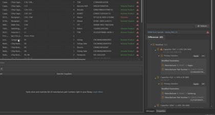
Save Time Looking at Differences in BOM CoDesign
You can now automatically exclude supplier related data from the differences section when comparing the engineering activeBOM with procurement BOMs managed in the BOM portal using BOM CoDesign.
Recommended Content:
- Visit the BOM CoDesign documentation page.
- Learn more about the Octopart Discover, Altium Develop, and Altium Agile platform solutions.
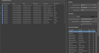
Protect Component Lifecycle States During Synchronization
A new Preserve lifecycle state option allows you to keep the existing lifecycle state when synchronizing components between your Workspace and your component database using the Components Synchronization feature.
Recommended Content:
- Learn more about the Octopart Discover, Altium Develop, and Altium Agile platform solutions.
Define Your Multi-board Terminations with Precision, Export a Complete Harness Excel Manufacturing Workbook, Validate Your 3D-MID Designs with Confidence
Define Your Multi-board Terminations with Precision
You can now define termination types directly in your multi-board schematics, with the ability to clearly specify if each harness entry connects to a connector, a crimp or ferrule, or a simple wire termination, giving you precise control over every connection.
Recommended Content:
- To see an overview visit the Multi-board Design feature page.
- Visit the Multi-board Design documentation page.
- Learn more about the Octopart Discover, Altium Develop, and Altium Agile platform solutions.
Export a Complete Harness Excel Manufacturing Workbook
You can export a complete Excel manufacturing workbook directly from your project This includes your BOM for quoting, wiring lists for automation, label summaries, and detailed covering information for assembly. Enhancements also include smarter wire validation, more flexible covering control, and clearer “As Required” material reporting for a smoother, more accurate manufacturing workflow.
Recommended Content:
- To see an overview about the Harness Design tool, visit the feature page.
- Visit the Harness Design documentation page.
- Learn more about the Octopart Discover, Altium Develop, and Altium Agile platform solutions.
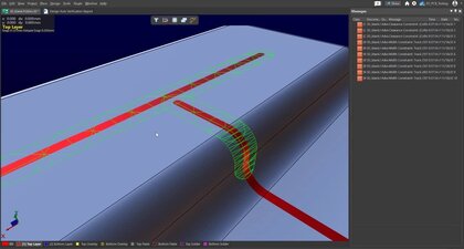
Validate Your 3D-MID Designs with Confidence
You can now run batch design rule checking for width, clearance, length, and matched lengths violations on all routed tracks on your 3D substrate.
Recommended Content:
- To see an overview about the 3D-MID Design Tool, visit the feature page.
- Visit the 3D-MID Design documentation page.
- Learn more about the Octopart Discover, Altium Develop, and Altium Agile platform solutions.
Altium Designer 25
Catch Your Syntax Issues Early for Custom Rules, Enhance Your Modular Design with Inline Harness Connectors, Speed Up Your Harness Drafting with Automatic Length Fills
What's New in Altium Designer 25.8
What's New in Altium Designer 25.8
Catch Your Syntax Issues Early for Custom Rules
The Constraint Manager now automatically detects and highlights any rule containing a syntactically incorrect custom query expression.
Recommended Content:
- To see an overview about the Constraint Manager, visit the feature page.
- Check out our recent OnTrack Podcast video on the Constraint Manager, Deep Diving Into Altium Designer's New Constraint Manager.
- Visit the Constraint Manager documentation page.
Enhance Your Modular Design with Inline Harness Connectors
The Inline Harness Connector feature in the multi-board schematic editor now allows you to divide an existing harness connection into two parts.
Recommended Content:
- To see an overview visit the Multi-board Design feature page.
- Check out our recent webinar on system design, Unlock Complete System Design with Altium Designer 24.
- Visit the Multi-board Design documentation page.
Speed Up Your Harness Drafting with Automatic Length Fills
The value field now automatically populates with the corresponding bundle length when you place a linear dimension between connection points in a harness manufacturing drawing.
Recommended Content:
- To see an overview about the Harness Design tool, visit the feature page.
- Check out our recent webinar on Harness Design, Future-Proof your Wire Harnesses with Altium Designer.
- Visit the Harness Design documentation page.
Boost Your Productivity with Automated Constraint Manager Refreshes, Accelerate Your Multi-Board Design with Collaborative Features, Simplify Your Workflow Through Grouped Component Operations
What's New in Altium Designer 25.7
What's New in Altium Designer 25.7
Boost Your Productivity with Automated Constraint Manager Refreshes
The Constraint Manager now automatically refreshes to import schematic directives when you push changes to the PCB using the Engineering Change Order (ECO) process.
Recommended Content:
- To see an overview about the Constraint Manager, visit the feature page.
- Check out our recent OnTrack Podcast video on the Constraint Manager, Deep Diving Into Altium Designer's New Constraint Manager.
- Visit the Constraint Manager documentation page.

Accelerate Your Multi-Board Design with Collaborative Features
There is now support for interactive commenting and task management in Multi-board Assembly documents.
Recommended Content:
- To see an overview visit the Multi-board Design feature page.
- Check out our recent webinar on system design, Unlock Complete System Design with Altium Designer 24.
- Visit the Multi-board Design documentation page.

Simplify Your Workflow Through Grouped Component Operations
All components are now organized under a new ‘Workspace Components’ folder in the Projects panel. This allows you to open, close, save locally, push to the Workspace, or discard changes for all grouped components at once.

Quickly Recover Your Edits in the Constraint Manager, Enhance Your Harness Design Accuracy and Visualization, Import Your Designs Seamlessly from Third-Party Tools
What's New in Altium Designer 25.6
What's New in Altium Designer 25.6
Quickly Recover Your Edits in the Constraint Manager
You now have the ability to Undo/Redo changes made within the Constraint Manager.
Recommended Content:
- To see an overview about the Constraint Manager, visit the feature page.
- Visit the Constraint Manager documentation page.

Enhance Your Harness Design Accuracy and Visualization
Parasolid format 3D models are now embedded in the layout drawing when adding a Physical View for a harness component or connection point.
Recommended Content:
- To see an overview about the Harness Design tool, visit the feature page.
- Check out our recent webinar on Harness Design, Future-Proof your Wire Harnesses with Altium Designer.
- Visit the Harness Design documentation page.
Import Your Designs Seamlessly from Third-Party Tools
When importing an xDX Designer design, a new option has been added that allows you to import 'off-page' connectors in the source design as ports on the generated schematic documents, rather than default off-sheet connectors.
Recommended Content:
- Visit the Import/Export documentation page to learn more.
Easily Synchronize Your Design Rules Across Projects, Efficiently Generate Your Differential Pairs from xNets, Achieve Greater Precision for Your Harness Coverings
What's New in Altium Designer
What's New in Altium Designer
Easily Synchronize Your Design Rules Across Projects
Advanced Rules with custom scopes can now be imported and exported from the Constraint Manager in Altium Designer. With this upgrade, all design rules can now be exported and imported using this functionality.
Recommended Content:
- To see an overview about the Constraint Manager, visit the feature page.
- Visit the Constraint Manager documentation page.

Efficiently Generate Your Differential Pairs from xNets
Differential pairs can now be generated from xNets using either the Physical view or the Diff Pairs tab of the Electrical view in the Constraint Manager.
Recommended Content:
- To see an overview about the Constraint Manager, visit the feature page.
- Visit the Constraint Manager documentation page.

Achieve Greater Precision for Your Harness Coverings
The Start offset and End offset can now be specified for a harness covering, which, combined with the enclosed bundle segment length, automatically calculates and displays the accurate covering length directly in the main design space and the BOM.
Recommended Content:
- To see an overview about the Harness Design tool, visit the feature page.
- Visit the Harness Design documentation page.

Simplify Routing with Automated Custom Topology and xSignal Creation, Ensure Comprehensive Documentation in Your Harness Designs, Efficiently Manage Layers When Importing Xpedition Files, Improve Organization and Accuracy Across Project Release Data
What's New in Altium Designer 25.4
What's New in Altium Designer 25.4
Simplify Routing with Automated Custom Topology and xSignal Creation
The Constraint Manager now automatically creates custom routing topologies and xSignals for xNets that traverse discrete components with more than two pins, such as resistor banks, upon selecting the Custom routing topology type.
Recommended Content:
- To see an overview about the Constraint Manager, visit the feature page.
- Visit the Constraint Manager documentation page.

Ensure Comprehensive Documentation in Your Harness Designs
In harness design, we’ve added the ability to specify Strip Length and Pull Off Length for pins lacking an assigned cavity type.
Recommended Content:
- To see an overview about the Harness Design tool, visit the feature page.
- Check out our recent webinar on Harness Design, Future-Proof your Wire Harnesses with Altium Designer.
- Visit the Harness Design documentation page.

Efficiently Manage Layers When Importing Xpedition Files
The import process for Mentor Xpedition files has been enhanced to allow toggling multiple layers on or off simultaneously during import.
Recommended Content:
- Visit the Import/Export documentation page to learn more.

Improve Organization and Accuracy Across Project Release Data
Defined project and variant parameters from your connected Workspace templates are now accurately used in naming released data sets such as Source, Fabrication, Assembly, and Custom outputs.
Recommended Content:
- Visit the Preparing Outputs and Releasing the Project documentation page to learn more.

Import Clearance Rules Automatically into the Clearance Matrix, Gain More Control Over Your Harness Design Settings, Generate and Place QR and Data Matrix Codes on your PCB
What's New in Altium Designer 25.3
What's New in Altium Designer 25.3
Import Clearance Rules Automatically into the Clearance Matrix
When importing clearance rules from schematic design directives or migrating projects from the legacy design rules dialog, clearance rules are now placed in the Clearance Matrix within the Constraint Manager, rather than being assigned to the Advanced Rules section.
Recommended Content:
- To see an overview about the Constraint Manager, visit the feature page.
- Check out our recent OnTrack Podcast video on the Constraint Manager, Deep Diving Into Altium Designer's New Constraint Manager.
- Visit the Constraint Manager documentation page.

Gain More Control Over Your Harness Design Settings
You now have more control over harness design settings. A new preference lets you set the default blank sheet size for wiring diagrams and layout drawings. Length units have been standardized and can be customized at different levels, including preferences, documents, and tables like BOMs and connection lists. You can also filter connection tables to show only 'no connect' objects. Additionally, a fix ensures that specified units now apply correctly to all wires, including those not part of a cable.
Recommended Content:
- To see an overview about the Harness Design tool, visit the feature page.
- Check out our recent webinar on Harness Design, Future-Proof your Wire Harnesses with Altium Designer.
- Visit the Harness Design documentation page to learn more.

Generate and Place QR and Data Matrix Codes on your PCB
You can now generate and place QR and Data Matrix codes directly in your PCB design, making it easier to add scannable data for tracking, identification, and automation.
Recommended Content:
- To learn more about PCB Layout in Altium Designer, visit the resource page.
- Visit the PCB Layout documentation page.

Use Qualified Models and Access Detailed Part Information, Make Automated xNets for Serial Component Pin Configurations, Generate an Intentional Shorts List with ODB++ v8.1 Support
What's New in Altium Designer 25.2
What's New in Altium Designer 25.2
Use Qualified Models and Access Detailed Part Information
Categorizes part models as 'Generic' or 'ECAD Ready,' with detailed model information available in the Manufacturer Part Search panel and related dialogs.
Recommended Content:
- Visit the Component Management documentation page to learn more.

Make Automated xNets for Serial Component Pin Configurations
Enhanced xNet generation for serial components automates the creation of xNets in the Constraint Manager based on the pin configurations of components, supporting dual-inline, single-inline, and odd-pin configurations.
Recommended Content:
- To see an overview about the Constraint Manager, visit the feature page.
- Check out our recent OnTrack Podcast video on the Constraint Manager, Deep Diving Into Altium Designer's New Constraint Manager.
- Visit the Constraint Manager documentation page.

Generate an Intentional Shorts List with ODB++ v8.1 Support
Adds support for generating a list of intentional shorts (Net-Ties) in ODB++ v8.1 output, including a new option in the ODB++ Setup dialog.

Enable Collaborative BOM Management with BOM CoDesign, Experience Clearer Terminology in the Auto Tuning Dialog, Export and Import Your Constraints with Unified Commands
What's New in Altium Designer 25.1
What's New in Altium Designer 25.1
Enable Collaborative BOM Management with BOM CoDesign
Through the Altium 365 Workspace, designers and procurement specialists can collaborate on related BOM snapshots, allowing for detailed comparisons between managed BOMs and the design’s ActiveBOM.
Recommended Content:
- Visit the BOM CoDesign documentation page.

Experience Clearer Terminology in the Auto Tuning Dialog
The Auto Tuning Process dialog has updated terminology, including “Tuning Goal” replacing “Pattern” and revised names for “Accordion” and “Sawtooth” to reflect their specific matching purposes.
Recommended Content:
- To learn more about PCB Layout in Altium Designer, visit the resource page.
- Visit the PCB Layout documentation page.

Export and Import Your Constraints with Unified Commands
The export and import processes for constraints and constraint sets have been streamlined into single commands.
Recommended Content:
- To see an overview about the Constraint Manager, visit the feature page.
- Check out our recent OnTrack Podcast video on the Constraint Manager, Deep Diving Into Altium Designer's New Constraint Manager.
- Visit the Constraint Manager documentation page.

Place Die Pads by Height with Wire Bonding Support, Use External Components in Your Multi-board Designs, Override the Calculated Wire Length in Your Layout Drawing, Design in Custom Components with Donut Pad Support, Ensure Accurate Variant Parameters for Seamless PLM Integration
What's New in Altium Designer 25.0
What's New in Altium Designer 25.0
Place Die Pads by Height with Wire Bonding Support
Die pads are now bound, by height, to the 3D body they are placed on instead of the highest 3D body in the die pad location.
Recommended Content:
- To see an overview, visit the feature page.
- Watch the recording of our recent webinar, Unlock New Design Possibilities with Wire Bonding.

Use External Components in Your Multi-board Designs
Multi-board design now has support for placing external peripherals/components that are not part of the regular child PCB board assemblies.
Recommended Content:
- To see an overview visit the Multi-board Design feature page.
- Check out our recent webinar on system design, Unlock Complete System Design with Altium Designer 24.
- Visit the Multi-board Design documentation page.

Override the Calculated Wire Length in Your Layout Drawing
Harness Layout Wire Length Override allows you to manually adjust the wire length on a Layout Drawing within a harness design.
Recommended Content:
- To see an overview about the Harness Design tool, visit the feature page.
- Check out our recent webinar on Harness Design, Future-Proof your Wire Harnesses with Altium Designer.
- Visit the Harness Design documentation page to learn more.

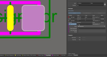
Design in Custom Components with Donut Pad Support
You can now create true round donut pad shapes in the properties panel.
Recommended Content:
- To learn more about PCB Layout in Altium Designer, visit the resource page.
- Visit the PCB Layout documentation page.

Ensure Accurate Variant Parameters for Seamless PLM Integration
Variant-level parameters defined in your project now correctly propagate into the assembly parameters upon release to your connected Workspace.

Altium Designer 24
Automatically Narrow Traces in Tight Spaces with Auto-shrinking, Simplify Chip-on-Board Design with Wire Bonding Support, Gain Insight with Harness and Multi-board View Only Mode, Ensure Signal Integrity with the SI Analyzer by Keysight
What's New in Altium Designer 24.10
What's New in Altium Designer 24.10
Automatically Narrow Traces in Tight Spaces with Auto-shrinking
The Auto-shrinking feature in the interactive router reduces the width of a trace to ensure it can be routed in tight spaces.
Recommended Content:
- To learn more about PCB Layout in Altium Designer, visit the resource page.
- Visit the PCB Layout documentation page.

Simplify Chip-on-Board Design with Wire Bonding Support
Wire Bonding Support allows for designing hybrid boards using chip-on-board (CoB) technology, enabling seamless integration of dies directly onto PCBs with bond wires connecting to other components.
Recommended Content:
- To see an overview, visit the feature page.
- Watch the recording of our recent webinar, Unlock New Design Possibilities with Wire Bonding.

Gain Insight with Harness and Multi-board View Only Mode
Harness & Multi-board View Only Mode in allows users with a Standard Subscription or Viewer License to access and explore Harness and Multi-board projects without editing rights.
Recommended Content:
- To see an overview visit the Harness Design and Multi-board Design feature pages.
- Check out our recent webinar on system design, Unlock Complete System Design with Altium Designer 24.
- Visit the Harness Design or Multi-board Design documentation pages.

Ensure Signal Integrity with the SI Analyzer by Keysight
This downloadable software extension allows you to perform signal integrity analysis directly within your design environment in Altium Designer.
Recommended Content:
- To see an overview, visit the product page.
- To see the Signal Integrity Analyzer in action, watch the video tutorials.
- Watch the recording of our webinar, Signal Integrity Made Simple.

Enable or Disable Rules Directly in the Constraint Manager, Release Your Harness Design Projects, Modify Tracks or Add New Vertices to Your 3D-MID Design
What's New in Altium Designer 24.9
What's New in Altium Designer 24.9
Enable or Disable Rules Directly in the Constraint Manager
Easily manage your PCB design rules with the ability to enable or disable basic rules directly from the All Rules view in the Constraint Manager from the PCB.
Recommended Content:
- To see an overview about the Constraint Manager, visit the feature page.
- Check out our recent OnTrack Podcast video on the Constraint Manager, Deep Diving Into Altium Designer's New Constraint Manager.
- Visit the Constraint Manager documentation page.

Release Your Harness Design Projects
Simplify your Harness Design release process with Altium Designer's Project Releaser. Automate and manage releases with one-touch ease, reducing errors and saving time, whether working online with Altium 365 or offline.
Recommended Content:
- To see an overview about the Harness Design tool, visit the feature page.
- Check out our recent webinar on Harness Design, Future-Proof your Wire Harnesses with Altium Designer.
- Visit the Harness Design documentation page.

Modify Tracks or Add New Vertices to Your 3D-MID Design
Refine your 3D-MID designs with Altium Designer's new track editing features. You can click and drag to modify tracks or add new vertices, giving you more control and precision in your design process.
Recommended Content:
- To see an overview about the 3D-MID Design Tool, visit the feature page.
- Visit the 3D-MID Design documentation page.

Set Layer-Specific Width Constraints from Your Schematic, Specify Strip and Pull Off Length for Your Crimps, Select and Drag Multiple Components in 3D-MID Design, Design Single-Layer PCBs with Integrated Layer Stack Management
What's New in Altium Designer 24.8
What's New in Altium Designer 24.8
Set Layer-Specific Width Constraints from Your Schematic
When accessing the Constraint Manager from the schematic, it is now possible to choose and configure specific width constraints per layer for any PCB document in the same design project, and independently across layer stacks defined for a chosen board.
Recommended Content:
- To see an overview about the Constraint Manager, visit the feature page.
- Check out our recent OnTrack Podcast video on the Constraint Manager, Deep Diving Into Altium Designer's New Constraint Manager.
- Visit the Constraint Manager documentation page.

Specify Strip and Pull Off Length for Your Crimps
You now have the ability to specify the 'Strip Length' and 'Pull Off Length' when defining a crimp-type cavity in the Wiring Diagram.
Recommended Content:
- To see an overview about the Harness Design tool, visit the feature page.
- Check out our recent webinar on Harness Design, Future-Proof your Wire Harnesses with Altium Designer.
- Visit the Harness Design documentation page.

Select and Drag Multiple Components in 3D-MID Design
3D-MID Design now includes the ability to select and drag multiple components on the substrate. This enhancement allows users to easily reposition multiple components simultaneously on the 3D substrate.
Recommended Content:
- To see an overview about the 3D-MID Design Tool, visit the feature page.
- Visit the 3D-MID Design documentation page.

Design Single-Layer PCBs with Integrated Layer Stack Management
The Single Layer PCB Support feature in Altium Designer allows users to create single-layer PCBs, with full integration in the Layer Stack Manager and related outputs.
Recommended Content:
- To learn more about Layer Stack Manager in Altium Designer, visit the documentation page.

Select Alternate Parts in Variants Without Changing Symbols, Import or Export Your Constraint Sets, Control Cavity Information in Connection Tables
What's New in Altium Designer 24.7
What's New in Altium Designer 24.7
Select Alternate Parts in Variants Without Changing Symbols
You now have the ability to choose alternate components in variants without changing the schematic symbol or PCB footprint.
Recommended Content:
- Visit the Schematic Capture documentation page.

Import or Export Your Constraint Sets
The Constraint Manager has been upgraded with features such as exporting/importing constraint sets, a global 'Ignore Pad to Pad clearance within a footprint' option, and improved rule cell highlighting within the PCB.
Recommended Content:
- To see an overview about the Constraint Manager, visit the feature page.
- Visit the Constraint Manager documentation page.

Control Cavity Information in Connection Tables
In Harness Design, you now have control over cavity information in Connection Tables. We’ve also added Commenting and Tasks features for collaborative reviews and task assignments.
Recommended Content:
- To see an overview about the Harness Design tool, visit the feature page.
- Check out our recent webinar on Harness Design, Future-Proof your Wire Harnesses with Altium Designer.
- Visit the Harness Design documentation page to learn more.

Place Components with Intricate Footprints for Your 3D MID Designs, Promote Favorite Filters for Your Components, Import KiCad Designs from Version 7 or 8
What's New in Altium Designer 24.6
What's New in Altium Designer 24.6
Place Components with Intricate Footprints for Your 3D MID Designs
Support for complex-shaped footprints and natural gridlines on 3D substrates, plus snapping priority override, makes designing easier and more efficient.
Recommended Content:
- To see an overview about the 3D-MID Design Tool, visit the feature page.
- Visit the 3D-MID Design documentation page.

Promote Favorite Filters for Your Components
Add favorite filters in the Manufacturer Part Search panel and preserve component lifecycle states when releasing new revisions for enhanced data management.
Recommended Content:
-
To see an overview about the Manufacturer Part Search, visit the feature page.
-
Visit the documentation page to learn about the searching and placing components.

Import KiCad Designs from Version 7 or 8
Ensure a smooth transition to Altium Designer and reduce manual tasks when importing your latest KiCad projects.
Recommended Content:
- Visit the Import/Export documentation page to learn more.

Import Values from Directives in the Constraint Manager, Create a Harness Design Template, Automatically Add a Supply Nets Rule, Generate the Latest V.8.1 ODB++ Format, Prevent Inadvertent Footprint Mirroring
What's New in Altium Designer 24.5
What's New in Altium Designer 24.5
Import Values from Directives in the Constraint Manager
Now, with a new dialog summarizing imported values from the schematic in the Constraint Manager, visualizing constraints becomes more intuitive. Additionally, imported directives are easily distinguished within the design space by their blue coloring and distinct symbols, with corresponding rules accessible in the properties panel. With support for creating xNets and xNet classes directly within the Constraint Manager from the PCB, bidirectional E-C-O propagation simplifies the synchronization between PCB and schematic sides. Furthermore, selecting the Custom topology for a 2-pin net automatically adds its pins as nodes to the topology editing area, facilitating quicker selection of proposed xSignals.
Recommended Content:
- To see an overview about the Constraint Manager, visit the feature page.
- To see the Constraint Manager in action, check out our recent webinar Empowering Faster Electronics Development with Altium Designer 24.
- Check out our recent OnTrack Podcast video on the Constraint Manager, Deep Diving Into Altium Designer's New Constraint Manager.
- Visit the Constraint Manager documentation page to learn more.

Create a Harness Design Template
You can create, upload, edit, and reuse Harness Wiring Diagram and Harness Layout Drawing templates within a connected Altium 365 Workspace, eliminating redundant efforts on your part. Additionally, Altium Designer offers enhanced control over your designs with the incorporation of a 'Type' field for objects in the Wiring Diagram and labels and coverings in the Layout Drawing, enabling precise management of their inclusion in the BOM. Moreover, shield objects can now be assigned a library ID, enhancing organization and accessibility. Simplifying wire color definition, Altium Designer now utilizes a single-color parameter in the Wiring Diagram, reflecting secondary and tertiary coloring for improved visibility and clarity. Furthermore, the introduction of an 'Include Cut' parameter for wire objects grants you control over their inclusion in a Wiring List placed in a Harness Draftsman document.
Recommended Content:
- To see an overview about the Harness Design tool, visit the feature page.
- Check out our recent webinar on Harness Design, Future-Proof your Wire Harnesses with Altium Designer.
- Visit the Harness Design documentation page to learn more.

Automatically Add a Supply Nets Rule
The 'Supply Nets' rule is automatically added to every power net during compilation.
Recommended Content:
- To see an overview about Schematic Capture, visit the feature page.
- Visit the Schematic Capture documentation page to learn more.

Generate the Latest V.8.1 ODB++ Format
You can now select between the latest ODB++ v.8.1 and legacy v.7.0 formats within a single installation. You can generate data for all defined variants collectively or separately, streamlining your workflow. Moreover, it simplifies Flex/Rigid-Flex manufacturing by incorporating various layer sub-types and implementing zones file support.

Prevent Inadvertent Footprint Mirroring
To help for early detection of footprint mirroring, 'No' is the default option in the warning dialog when using a keyboard shortcut to flip a component or room to add a layer of safety. There is also a new check ‘Components with Mirrored Footprints’ option added to the Components section of the PCB Health Check Monitor, which detects changes in pins between a placed component footprint in the PCB design space and the corresponding footprint in the applicable source library. Additionally, the 'Update From PCB Libraries' tool has been enhanced to detect changes in designators and 3D bodies across all layers, with differences listed on the Properties tab.
Recommended Content:
- To learn more about PCB Layout in Altium Designer, visit the resource page.
- Visit the PCB Layout documentation page.

Automatically Propagate Width Values in the Constraint Manager, Remove Polygon Necks Less Than a Specified Width, See the Exact YTEOL Value for Your Components
What's New in Altium Designer 24.4
What's New in Altium Designer 24.4
Automatically Propagate Width Values in the Constraint Manager
You can now enter a width value into a single cell at the top grid area, and it will automatically propagate to all corresponding width or gap fields. Furthermore, when working from a schematic, there is an indication of the sync status between constraints defined in the Constraint Manager and those specified through design directives in the source schematics.
Recommended Content:
-
To see an overview about the Constraint Manager, visit the feature page.
-
To see the Constraint Manager in action, check out our recent webinar Empowering Faster Electronics Development with Altium Designer 24.
-
Check out our recent OnTrack Podcast video on the Constraint Manager, Deep Diving Into Altium Designer's New Constraint Manager.
-
Visit the documentation page to learn about the Constraint Manager.
-
Discover the latest features and capabilities of Altium Designer 24 with free training.

Remove Polygon Necks Less Than a Specified Width
With the new "obey rules" option in the properties panel, you now have the capability to remove necks less than a specified width for placed polygon pours. Furthermore, Altium Designer now observes user-defined geometries for the component selection bounding box when moving a component in Push Obstacles mode.
Recommended Content:
-
Visit the documentation page to learn about PCB Layout.
-
Discover the latest features and capabilities of Altium Designer 24 with free training.

See the Exact YTEOL Value for Your Components
The real value for years to end of life parameter is accurately displayed across all instances where SiliconExpert data is presented, ensuring clarity and precision in your design process. Additionally, we’ve added support for referencing SiliconExpert compliance datasheets, enhancing accessibility and usability. We’ve also included support for the newest Microsoft Access Database file format when synchronizing Database to Workspace components.
Recommended Content:
-
To see an overview about the Manufacturer Part Search, visit the feature page.
-
Visit the documentation page to learn about the searching and placing components.
-
Discover the latest features and capabilities of Altium Designer 24 with free training.

Ensure Accurate Electrical Clearances with the Constraint Manager, Specify Details for Each Pin of Your Harness Component, Utilize S-Parameters to Characterize Your Networks
What's New in Altium Designer 24.3
What's New in Altium Designer 24.3
Ensure Accurate Electrical Clearances with the Constraint Manager
A Creepage rule can now be specified for electrical clearances between nets and/or differential pairs, facilitated by the matrix in the Clearances view. Also, support has been added to the clearance matrix for multi-editing within a selected row or column to streamline your workflow.
Recommended Content:
-
To see an overview about the Constraint Manager, visit the feature page.
-
To see the Constraint Manager in action, check out our recent webinar Empowering Faster Electronics Development with Altium Designer 24.
-
Check out our recent OnTrack Podcast video on the Constraint Manager, Deep Diving Into Altium Designer's New Constraint Manager.
-
Visit the documentation page to learn about the Constraint Manager.
-
Discover the latest features and capabilities of Altium Designer 24 with free training.

Specify Details for Each Pin of Your Harness Component
You now have the ability to specify crimps, seals, plugs, or other cavity parts for each required pin directly within the Wiring Diagram. These elements are also seamlessly integrated into the wiring list and connection table in the Draftsman document, providing clarity and precision to your designs.
Recommended Content:
-
To see an overview about Harness Design, visit the feature page.
-
Visit the documentation page to learn about Harness Design.
-
Discover the latest features and capabilities of Altium Designer 24 with free training.

Utilize S-Parameters to Characterize Your Networks
Altium Designer’s S-parameters tool, available within the Simulation Dashboard panel, offers a method to characterize networks by evaluating the ratio of incident and reflected microwaves, effectively addressing challenges in high-frequency circuits.
Recommended Content:
- Witness the benefits of using the Simulation tool in this short video.
- To see an overview about the Simulation tool, visit the feature page.
- Visit the documentation page to learn about the Simulation tool.
- Discover the latest features and capabilities of Altium Designer 24 with free training.

Transfer Design Constraints Between your PCB and Schematic, Set Multiple Colors to a Wire in your Harness Design, Manually Map Components with PCB Layout Replication
What's New in Altium Designer 24.2
What's New in Altium Designer 24.2
Transfer Design Constraints Between your PCB and Schematic
When accessing the Constraint Manager from the PCB editor and defining constraints on the Physical and Electrical views, it is now possible to transfer those constraints to the Schematic through the Engineering Change Order (ECO) process. This enhancement ensures design consistency by reducing errors and saving time in the constraint definition process.
Recommended Content:
- To see an overview about the Constraint Manager, visit the feature page.
- To see the Constraint Manager in action, check out our recent webinar Empowering Faster Electronics Development with Altium Designer 24.
- Check out our recent OnTrack Podcast video on the Constraint Manager, Deep Diving Into Altium Designer's New Constraint Manager.
- Visit the Constraint Manager documentation page to learn more.

Set Multiple Colors to a Wire in your Harness Design
Altium Designer has added support for multi-colored wires, with the ability to define primary, secondary, tertiary, and border colors as part of a wire's parameters to help expand the functional identification capability of wires in your design.
Recommended Content:
- To see an overview about the Harness Design tool, visit the feature page.
- Check out our recent webinar on Harness Design, Future-Proof your Wire Harnesses with Altium Designer.
- Visit the Harness Design documentation page to learn more.

Manually Map Components with PCB Layout Replication
You now have the ability to manually map components in target blocks where multiple components have been detected by the PCB Layout Replication Tool as having similar connections. This allows you to manually choose between available components that are able to replace each other, without violating circuit connectivity.
Recommended Content:
- Witness the benefits of using the PCB Layout Replication tool in this short video.
- To see the PCB Layout Replication in action, check out our demonstration video.
- Visit the PCB Layout Replication documentation page to learn more.

Experience a Heightened Level of Control with the Constraint Manager, Highlight Specific Modified Categories with PCB CoDesign, Create a Clear Visual Representation of your Multi-Board Project, Make Informed Component Decisions with Stress Analysis
What's New in Altium Designer 24.1
What's New in Altium Designer 24.1
Experience a Heightened Level of Control with the Constraint Manager
Altium Designer's Constraint Manager, with significant enhancements in design control, is now more flexible and intuitive. Efficiency in design organization is improved with the capability of adding nets to an existing class. Custom topologies are defined more insightfully with structured xSignals, and we’ve also added line numbers on tabs/grids to enhance clarity and navigation. Lastly, you can now choose between the Constraint Manager and the older Design Rules system when creating a new project to adapt to your preferred workflow.

Highlight Specific Modified Categories with PCB CoDesign
Altium Designer's latest PCB CoDesign enhancements offer a more efficient and streamlined collaboration process. You can now precisely compare and apply changes to unions for targeted modifications. Also, the ‘Show on PCB’ option simplifies highlighting changes in specific categories for better visualization. These improvements aim to boost efficiency and provide a more organized and seamless collaborative design experience.

Create a Clear Visual Representation of your Multi-Board Project
Altium Designer's Multi-board Draftsman tool integrates manufacturing drawings into Multi-board design projects. The multi-board view displays combined graphics of PCB outlines and 3D models with various viewing options. Enjoy standard Draftsman features like annotation, dimensioning, and BOM, and say goodbye to managing different documentation sets or relying solely on MCAD software. Draftsman for Multi-board offers a clear visual representation of board connections in larger systems, ensuring design integrity and consistency.

Make Informed Component Decisions with Stress Analysis
Altium Designer introduces the Simulation Stress Analysis tool, which enhances the design process by incorporating stress analysis within transient analysis. This tool calculates and checks component operating conditions against defined limits, simplifies stress model creation, and allows for reliability derating. With a comprehensive stress chart in the simulation viewer, it provides precision and control for informed decisions on component reliability and performance.

Simplify Complex Design Rules with the Constraint Manager, Work Together and Design Faster with PCB CoDesign, Elevate Your Projects with the 3D Mechatronic Integrated Device Tool, Assign Currents to Multiple Nets with the Power Analyzer by Keysight
What's New in Altium Designer 24.0
What's New in Altium Designer 24.0
Simplify Complex Design Rules with the Constraint Manager
Altium Designer's Constraint Manager, available for pro and enterprise subscriptions, simplifies meeting complex standards and PCB design requirements. This tool allows easy browsing, creation, modification, and reuse of verified constraint sets through a tabular, object-based user interface. Enhancing clarity and comprehension, it seamlessly integrates rules between schematics and PCB layout, streamlining the design process with a consistent format for rule addition in both areas.

Work Together and Design Faster with PCB CoDesign
Altium Designer's PCB CoDesign simplifies collaboration, ensuring design integrity for engineering teams. With pro and enterprise subscriptions, this tool streamlines cooperation within your workspace, eliminating manual change tracking. Visualize alterations, compare layouts, and merge updates effortlessly in a unified environment. Say goodbye to cumbersome revision histories and embrace a more efficient PCB design approach with PCB CoDesign.

Elevate Your Projects with the 3D Mechatronic Integrated Device Tool
Altium Designer introduces the groundbreaking 3D Mechatronic Integrated Device design tool, simplifying the integration of non-planar electronic designs. It seamlessly aligns with existing components, synchronizes with schematic documents, and eliminates the need for time-consuming M-CAD hacks. This tool meets electrical specifications while enabling aesthetically pleasing designs. With pro or enterprise subscriptions, it facilitates easy adoption in your product development workflow.

Assign Currents to Multiple Nets with the Power Analyzer by Keysight
Altium Designer's enhanced Power Analyzer by Keysight Tool addresses power network analysis challenges efficiently. With new support for assigning currents to multiple nets on the same component across different series elements. This enhancement ensures a seamless and efficient power analysis experience, allowing you to maximize benefits from your design in Altium Designer.

Altium Designer 23
Tackle Any Design Complexity With the Constraint Manager, Speed Up Your Workflow With the Power of PCB Layout Replication, Minimize Manual Effort With Automatic Length Tuning
What's New in Altium Designer 23.11
What's New in Altium Designer 23.11
Tackle Any Design Complexity With the Constraint Manager
For enterprise and pro subscriptions, the new Constraint Manager offers a table-based interface, accessible from both Schematic and PCB, allowing you to define constraints more collaboratively. Engineers and stakeholders can collectively set design constraints with ease.

Speed Up Your Workflow With the Power of PCB Layout Replication
The new PCB Layout Replication tool gives you the ability to quickly replicate the layout for repetitive blocks of circuitry in a flat PCB design. This avoids the need for manual routines, snippets, reuse blocks, or converting into a multi-channel design.

Minimize Manual Effort With Automatic Length Tuning
Automatic Length Tuning introduces automatic length and delay tuning functionality in 2D mode, accessed conveniently from the main Route menu. This feature reduces the manual effort typically associated with length and delay tuning, expediting your design process.

Easily Edit Paste and Solder Mask Shapes, Retrace Single-Ended Traces at any Angle, Track Components in Reuse Blocks with the “Where Used” Panel, Efficient Concurrent Design with PCB CoDesign
What's New in Altium Designer 23.10
What's New in Altium Designer 23.10
Easily Edit Paste and Solder Mask Shapes
The custom paste and solder mask feature is now automatically enabled by default, allowing you to personalize pad shapes directly without the need for workarounds. This simplification improves manufacturing efficiency, project clarity, and provides a more user-friendly interface.

Retrace Single-Ended Traces at any Angle
We've added a new "Retrace Parameters" feature to the Gloss and Retrace panel, offering enhanced flexibility for retracing single-ended traces at any angle using the Rounded hugging style. You can also set rule-based width modes or input custom values to ensure compliance with design rules. Furthermore, you have the option to "Preserve Route Path," allowing you to maintain precise trace geometry during retracing, providing greater control and design accuracy.

Track Components in Reuse Blocks with the “Where Used” Panel
Altium Designer's "Where Used" component panel streamlines component management in your PCB designs. It offers a comprehensive list of where each component is used, making conflict resolution and maintaining design accuracy a breeze. The latest enhancement features a redesigned panel and integration of Reuse Blocks from the connected Workspace's library, with tabs displayed only when relevant to reduce clutter.

Efficient Concurrent Design with PCB CoDesign
For Pro and Enterprise subscriptions, PCB CoDesign in Altium Designer revolutionizes collaborative design by enabling multiple team members to work simultaneously on a project, ensuring streamlined development, efficient testing, and faster iteration to meet project deadlines. This feature includes Git-like version control, allowing collaborators to access the same project concurrently, commit changes to a master branch, and use Commenting and Tasks features to allocate work on the board. Notifications alert team members of commits, and the Compare and Merge panel displays differences in design, offering color-coded feedback. When conflicts arise, such as overlapping changes by multiple designers, you can confidently decide to keep local changes or accept remote changes from the latest commit, ensuring a smooth collaborative design process.

Seamlessly Import OrCAD and Allegro Design Files, Migrate Projects from SVN to Git in Your Enterprise Server Workspace, Optimize License Management with Enhanced Navigation and Labels, Unlock More Efficient Harness Design Features and Easily Validate Projects
What's New in Altium Designer 23.9
What's New in Altium Designer 23.9
Seamlessly Import OrCAD and Allegro Design Files
There are key improvements and fixes in relation to the import of OrCAD and Allegro design files into Altium Designer. This includes support for customized port connectors, accurate title block parameter handling, component fill coloring preservation, and precise design file imports, ensuring your design process is seamless.

Migrate Projects from SVN to Git in Your Enterprise Server Workspace
For enterprise, when connected to an Enterprise Server Workspace and a design project is stored in a SVN repository managed through the Workspace's Version Control Service, you can now migrate this project from the SVN repository to the Workspace's built-in Git repository.

Optimize License Management with Enhanced Navigation and Labels
When it comes to license management, the search field and related sorting control will now appear only when more than seven licenses are in the listing to avoid redundancy. Also, license type labels have been added to help quickly distinguish differences between licenses in the listing.

Unlock More Efficient Harness Design Features and Easily Validate Projects
For Harness Design, the zoom level now sets the size of the model view's green box automatically. No need for manual adjustments. We've also added quick keyboard shortcuts for adding wires and placing bundles to streamline your workflow. Plus, you can easily validate your active harness project with the new validate button.

Simply Copy Room Format with Rotation, Add New Special Strings for Fabrication and Assembly Notes, Freely Customize Paste Mask and Solder Mask
What's New in Altium Designer 23.8
What's New in Altium Designer 23.8
Simply Copy Room Format with Rotation
There is a new functionality of the ‘Copy Room Formats’ feature with the addition of an option to control whether or not the rotation of the chosen source room is copied to the desired destination room, avoiding the need for manual rotation corrections.

Add New Special Strings for Fabrication and Assembly Notes
You can now include a wider range of manufacturing and assembly parameters, such as layer counts, board dimensions, and object quantities directly into your fabrication and assembly notes. These additions are conveniently auto-calculated directly from the PCB, ensuring that your notes align with any design updates.

Freely Customize Paste Mask and Solder Mask
Altium has completed the custom pad stack feature, which includes the ability to freely customize pad, thermal relief, and most recently, paste and solder mask shapes. You now have the ability to independently control paste and solder mask shapes and can adapt to non-standard component footprints.

Conveniently Manage Part Choices for Each Component in Your Design, Precisely Measure your Results with the New Simulation Data Viewer, Easily Keep Track of your Harness Wiring Diagrams
Conveniently Manage Part Choices for Each Component in Your Design
Altium has added the ability to manage part choices that are associated with each component in your design. The excluded part choice will still be in the project, however it will not appear in the generated BOM, nor will it be used in price calculations or as part of BOM checks

Precisely Measure your Results with the New Simulation Data Viewer
The new Mixed-Simulation Data Viewer introduces higher waveform accuracy and measurement precision. This extended precision significantly reduces the likelihood of round-off errors, ensuring more accurate results when viewing simulation waveforms to improve the overall reliability of the simulation process.

Easily Keep Track of your Harness Wiring Diagrams
Altium has expanded support for additional multi-board features, which allows you to navigate to your wiring diagrams seamlessly from your multi-board schematic. You are now able to cross-probe directly from the corresponding harness object on the multi-board schematic to the Wiring Diagram of that harness design, minimizing the risk of mismatch and giving you more control over your multi-board design.

Precisely Position Silkscreen for Footprint Creation and PCB Manufacturing Preparation , Utilize the FSTIM Stimulus Model During Simulation, Create Your Harness Cable Assembly Drawing Even More Precisely
What's New in Altium Designer 23.6
What's New in Altium Designer 23.6
Precisely Position Silkscreen for Footprint Creation and PCB Manufacturing Preparation
The latest release simplifies the management of the silkscreen preparation process, offering the ability to effortlessly move or clip silkscreen objects at specific distances from exposed copper or solder mask openings. This eliminates the need for manual silkscreen work while creating footprints and PCB manufacturing preparation.

Utilize the FSTIM Stimulus Model During Simulation
Altium's latest release adds simulation capabilities by providing expanded support for additional components. You are now able to add your digital file stimulus device (FSTIM) model primitives from PSpice for simulation in Altium to achieve high accuracy and efficiency in generating transient signals. This addition aligns with Altium's ongoing commitment to have a best-in-class SPICE simulator fully integrated within the Altium Designer environment.

Create Your Harness Cable Assembly Drawing Even More Precisely
This release introduces new tools for precise harness cable design, helping to reduce errors during assembly. You can now define the size of the harness covering relative to the enclosed bundle and choose between solid-style and patterned fills. Additionally, isometric views in the Layout Drawing give assemblers an additional viewpoint to enhance the presentation of harness components, enabling comprehensive communication of design intent and minimizing assembly errors.

Discover the hidden parts of your board with the pcb section view, Custom Thermal Reliefs for Pads, Test Your Circuits With Real-Time Simulation Probes
What's New in Altium Designer 23.5
What's New in Altium Designer 23.5
Discover the hidden parts of your board with the pcb section view
The PCB section view provides precise insight into the layout and structure of your designs, like never before. when working with dense and complex PCBs the section view reveals the details within a PCB that are typically not visible. With full control over plane placement and color you can easily see all components, even smaller SMD components hiding under larger components or mechanical parts.

Custom Thermal Reliefs for Pads
As a continuation of our custom pad shape capabilities, it is now possible to add, remove, and edit, thermal relief spikes to anywhere on a pad, regardless of shape. This helps with soldering and avoids possible manufacturing problems like tombstoning.

Test Your Circuits With Real-Time Simulation Probes
The interactive probes feature is like using an oscilloscope right within Altium Designer. When this feature is enabled, any changes to probe placement, color, or other settings, are immediately reflected in the simulation results document.

Circuit Simulation support for Output Values in AC Analysis for Controlled Sources and Variable Passives, Live Traces & Fixed Aspect Ratios for Harness Wiring Diagram Objects, New in Harness Design: 3D wireframe View And Ability to Add Models to Connection Points
What's new in Altium Designer Release 23.4
What's new in Altium Designer Release 23.4
Circuit Simulation support for Output Values in AC Analysis for Controlled Sources and Variable Passives
We’ve now added support for voltage and current controlled sources, functional sources and variable passive components for voltage, power and current output variables in the AC analysis. Great for audio projects, communication designs, and other design types. Plus we’ve added support for multi-bit ADC and ROM PSPICE digital model primitives as well as their timing models.

Live Traces & Fixed Aspect Ratios for Harness Wiring Diagram Objects
Live traces actively follow your cursor, showing you the way to your final wire destination. Allowing you to move more efficiently in the wiring diagram. Wiring diagram objects are now synced with the documents snap grid, bringing a new level of uniformity to the diagram.

New in Harness Design: 3D wireframe View And Ability to Add Models to Connection Points
In the Layout Drawing, it is now possible to show the Physical (3D) model for a connector as a wireframe view and also, for a connection point, display the Physical (3D) model of one of its associated parts.

Support For Workspace Defined Parameters & Bulk Edits For Components, Added Support for Variable Passives & Global Nodes, Harness Design Improvements
Support For Workspace Defined Parameters & Bulk Edits For Components
For this release we have added support for workspace defined project parameters, bulk creation and edits of components, and enhanced side-by-side component revision comparison.

Added Support for Variable Passives & Global Nodes
This release of Altium Designer we’ve added support for more programmable logic array PSPICE digital primitives as well as support for digital models that use global nodes ($D_HI, $D_LO, $D_X), and variable passives.

Harness Design Improvements
The wiring diagram and layout drawing for harness projects has been given several new features to boost usability. We’ve added additional crimping capabilities, scaling options for documentation, visual connection lines for components and more.

Gerber Setup Layer Class Support, Added Support for PSpice Digital models, Harness Design Improvements
What’s new in Altium Designer Release 23.2
What’s new in Altium Designer Release 23.2
Gerber Setup Layer Class Support
The Gerber Setup dialog now includes a Layer Classes section in its Layers to plot list. Using the checkbox for layer classes, you can quickly enable plotting for all the layers that belong to a specific layer class.

Added Support for PSpice Digital models
This release of Altium Designer supports even more PSPICE digital model primitives. We’ve added support for the PINDLY, and CONSTRAINT Pspice digital behavioral model primitives as well as support for the DIGRRGEFAULT option.

Harness Design Improvements
In this release of Altium Designer we’ve added several new features to boost the usability of the harness wiring diagram and layout drawing. Including additional features for crimping, splices, and efficiency

Update to Collaboration and Reporting, Additional Harness Design Capabilities, New PCB Capabilities for Gerber and View Configuration
What’s new in Altium Designer Release 23.1
What’s new in Altium Designer Release 23.1
Update to Collaboration and Reporting
To better convey a message to other project stakeholders, you now have the capability to copy and paste pictures into your comments. Also, exporting a project history report can now be easily done through the Reports menu.

Additional Harness Design Capabilities
This release has added several improvements for both the harness wiring diagram and the Harness layout drawing. Some new capabilities include: parameters for twist and shield objects, crimping, additional 3D views, multiple connections from a single point and more…

New PCB Capabilities for Gerber and View Configuration
New PCB features allow you to load a stored view configuration file from the View Configuration Panel. Also, it is now possible to change the name for the Gerber Board Profile layer when using the new, unified Gerber/Gerber X2 dialog.

New Extension For Power Integrity Analysis, Multi-board support In MCAD CoDesigner, New Harness Design Capabilities
What’s new in Altium Designer Release 23.0
What’s new in Altium Designer Release 23.0
New Extension For Power Integrity Analysis
Quickly assess the integrity of your power distribution network without the need for any specialized training with Power Analyzer by Keysight.

Multi-board support In MCAD CoDesigner
You are now able to transfer and sync your muli-board designs with your mechanical team using the MCAD CoDesigner.

New Harness Design Capabilities
Harness Design functionality allows you to create a full wiring harness design, from the individual pin-to-pin connections right through to manufacturing documentation.

Altium Designer 22
Custom Pad Shapes with Rounded/Chamfered Corners, Enhanced Gerber Setup Interface, Additional Digital Models & Variant Support
What’s new in Altium Designer Release 22.11
What’s new in Altium Designer Release 22.11
Custom Pad Shapes with Rounded/Chamfered Corners
Shape your pads the way you need in a matter of clicks. Extending the versatility of pad shapes, you can now customize the rounding of selected corners of pads that use either the Rounded Rectangle shape or the new Chamfered Rectangle shape.

Enhanced Gerber Setup Interface
Efficiency, simplicity and convenience are all delivered with the new UI for Gerber setup. Everything you need to prepare for Gerber generation is now at your fingertips in an intuitive setting.

Additional Digital Models & Variant Support
Expanding the functionality available to you in the simulation arena, this release adds further support for PSPICE digital gates, timing and I/O models. Support for variants is also now available.

Improved Manufacturer Part Search UI, Additional Net Information for Tuning Objects, Quickly View Multi-function Pin Names
What’s new in Altium Designer Release 22.10
What’s new in Altium Designer Release 22.10
Improved Manufacturer Part Search UI
The Manufacturer Part Search panel has long been a source of components for many users. Improvements have been made in this release that make it easier to use components in their libraries. This allows you to spend more time on development than on the process!

Additional Net Information for Tuning Objects
Detailed net information about tuning objects has been added in this release. Information about the maximum current and active resistance of accordion, sawtooth, and trombone objects is now available. More detail means it is less likely mistake will be made!

Quickly View Multi-function Pin Names
A large number of microcircuits have multi-functional pins. Working with them in Altium Designer has become even easier. This release introduces the ability to display the alternative pin names with just one click.

Improved Variant Management, BOM Commenting, Alternative PCB Layouts in a Reuse Block
What’s new in Altium Designer Release 22.9
What’s new in Altium Designer Release 22.9
Improved Variant Management
Variant management is taken to the next level with this release. Time spent creating and editing variants is greatly reduced. Now you can design with large numbers of variants with streamlined ease and efficiency.

BOM Commenting
Support for commenting has arrived in the BOM arena with this release. All stakeholders can actively discuss the BOM with ease and convenience, as enjoyed already with schematic and PCB documents.

Alternative PCB Layouts in a Reuse Block
Reuse Blocks are enhanced further in this release. You can now define multiple, alternate PCB layouts for use with a single block. When placing a block, quickly switch layouts to suit your physical and performance needs.

Design Reuse Functionality, Mark Multiple Components as Fitted/Not Fitted, Custom Pad Shapes
What’s new in Altium Designer Release 22.8
What’s new in Altium Designer Release 22.8
Design Reuse Functionality
Take the enhanced functionality of Reuse Blocks for a spin in this release, with the ability to place a block (or schematic snippet) as a sheet symbol. Your proven circuitry is placed on an auto-generated child sheet.

Mark Multiple Components as Fitted/Not Fitted
With this release it becomes even easier to work with multi-variant design projects. Now you can select multiple components for the active variant and mark them as Fitted/Not Fitted in a single action.

Custom Pad Shapes
Modern components often contain pads that are complex in shape. This release of Altium Designer gives you the ability to create custom pad shapes quickly and easily, with management similar to that of standard pads.

Ability to Change Tuning Object Layer Properties, Auto-assign Simulation Models for Components without Models, Control of Paste Mask Output for Variants
What’s new in Altium Designer Release 22.7
What’s new in Altium Designer Release 22.7
Ability to Change Tuning Object Layer Properties
Design of high-speed PCBs becomes easier with this latest release. Now, when you need to quickly move tuning elements to a different layer, you can do so from the Properties panel with a single click.

Auto-assign Simulation Models for Components without Models
This latest version of Altium Designer makes schematic simulation even easier. System intelligence automatically recognizes SPICE models and assigns them to components from available sources.

Control of Paste Mask Output for Variants
Output data needs to be as accurate as possible. For multi-variant designs you can now ensure that the paste mask is only displayed where it is really needed.

Quick Browsing of Parameters for a Board, Active Links in Text, Multifunctional pins
What’s new in Altium Designer Release 22.6
What’s new in Altium Designer Release 22.6
Quick Browsing of Parameters for a Board
Parametric information for your board is now conveniently available from the Properties panel. A single, convenient location with which to browse system, calculated and user-defined parameters, and place as needed in the form of special strings.

Active Links in Text
You can now specify active links to components and nets within a text frame object on a schematic. This handy navigation aid makes it much easier not only to read the document, but also to work with it.

Multifunctional pins
You will often see that modern ICs consist of multi-functional pins. In this latest version of Altium Designer it has become far easier and much more convenient to work with such components.

Custom Diff Pair Suffixes, PCB Health Check Monitor
What’s new in Altium Designer Release 22.5
What’s new in Altium Designer Release 22.5
Custom Diff Pair Suffixes
Even more possibilities for creating differential pairs. Now you can use any postfixes to designate positive and negative net of a differential pair.

PCB Health Check Monitor
The condition of the PCB is under your control. A new intelligent feature that gives you confidence that your PCB is okay and complies with design rules.

Display of Alternate Component Parameters, Components from Altium 365, New Design Reuse Functionality
What’s new in Altium Designer Release 22.4
What’s new in Altium Designer Release 22.4
Display of Alternate Component Parameters
Many schematic solutions are created as multivariant. With the new release, the schematic of multivariant project have become even more detailed and informative.

Components from Altium 365
Working with multiboards has become easier and more convenient. Now you have more component sources at your disposal.

New Design Reuse Functionality
A reuse bloks help reduce development time and avoid errors. The new Design Reuse Panel and new functionality expands the possibilities for reuse blocks and snippets.

Schematic Capture Improvement, Relative Length Tuning, Enhanced UI for Via Stack Editing, Generic Components
What’s new in Altium Designer Release 22.3
What’s new in Altium Designer Release 22.3
Schematic Capture Improvement
Adding cross-references to the project allows you to easily follow the connective flow of nets between the schematic sheets in a project.

Relative Length Tuning
Designing high-speed PCB just got easier. The Length Tuning tools is now even more functionality. Complex tasks can now be solved even faster.

Enhanced UI for Via Stack Editing
The via editing mode is now even more convenient. Information about the via, editing its parameters and connections to polygons are now all in a new and simple, but familiar form.

Generic Components
The way from idea to real devices has become shorter. The new feature will reduce the time it takes to design a schematic.
