Welcome, Guest

Sign in to learn, create, and do more with the product you love.

News & Updates

Filters:
Tag
Blog
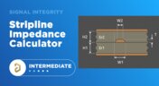
Stripline Impedance Calculator

Striplines provide some advantages over microstrips as they take advantage of natural shielding and coupling from nearby ground plane layers. Although they tend to experience higher losses due to total confinement in the dielectric, they can be thinner due to the high dielectric constant used in internal layers of a PCB. Use our free impedence calculator to help you determine the correct width needed to hit a target impedance.

Embedded thumbnail for Query Language: What is It For?
How-To's
Query Language: What is It For?

A PCB project contains many different objects. How to manage them? How to find the right ones quickly and efficiently? This video starts the series about query language. Learn the language commands and how to use them and expand your possibilities!

Blog
Which Types of Opto-Isolators Are Right For Your Signal?

An optoisolator is a cool electronic device that can be used to pass information between a diode without passing an electrical current. There are many great applications for these, but do you know which one is right for you?

Blog
Properties panel document options in SCH editors

The Properties panel provides access to the properties of documents and objects. The contents of the panel change depending on the active document or the selected object. This blog will quickly go over some of need to know options around the properties panel in the schematic document.

Embedded thumbnail for PCB design with BGA: Via-in-Pad
How-To's
PCB design with BGA: Via-in-Pad

We’ll teach you how to use Via-in-pad to reduce inductance, improve signal integrity, and improve power distribution system performance.

Embedded thumbnail for Design RF PCB: Distributed-Element Circuits
How-To's
Design RF PCB: Distributed-Element Circuits

Distributed-element circuits are a topology of a particular shape and size. Filters, power dividers, directional couplers can be built from them. Being calculated in third-party CAD, the topology of such elements can be easily imported into Altium Designer, and we will show you how to do it!

Embedded thumbnail for How to work with components on a rigid-flex board in MCAD
How-To's
How to work with components on a rigid-flex board in MCAD

With MCAD Codesigner you can quickly add and move components from your MCAD tool and update the design automatically in Altium Designer. We’ll show you how to. Add a new component, move components, and change a component’s region in MCAD, and update it to your design in Altium Designer.

Embedded thumbnail for LSM: Impedance profile
How-To's
LSM: Impedance profile

Creating Impedance profiles for transmission lines and how to apply them to the board

High-Speed PCB Stackup Design
Blog
The High-Speed PCB Stackup Design Challenge

Even with all the good guidelines out there for high speed design, there are particular aspects of stackup construction and their relation to building boards that get overlooked. This blog is goes beyond just the typical SI/PI guidelines and looks at these problems from more of an engineering perspective.

Embedded thumbnail for Multichannel Schematic: Creating Channels
How-To's
Multichannel Schematic: Creating Channels

Altium Designer makes creating single and multichannel designs effective and quick. We’ll show you how to create and annotate output and input channels in your design.

Embedded thumbnail for How to efficiently use Blankets?
How-To's
How to efficiently use Blankets?

Blanket is a powerful tool for group assignment of properties in schematic documents. It makes it easier and faster to assign circuit classes, differential pairs, and design rules within schematic documents. This video provides instructions on how to use blanket to simplify work in your designs.

stitching vias
Blog
Everything You Need to Know About Stitching Vias

Stitching vias are something you often see spread around the surface layer of a PCB, but what are they? and should you be using them? In this guide, we'll go over some of the standard uses of stitching vias and when they should be used in a PCB.

Embedded thumbnail for High Speed: XSignals for DDR3/DDR4
How-To's
High Speed: XSignals for DDR3/DDR4

In high speed design DDR3 and DDR4 memory chips can utilize xSignal classes to match track lengths from the controller to the memory chip easily and quickly. We’ll show you how using the xSignals wizard.

Embedded thumbnail for Design RF PCB: routing (any angle, arc)
How-To's
Design RF PCB: routing (any angle, arc)

It is worth taking a responsible approach to the shape and size of the RF signal conductors. In this video we will cover some practical aspects of working with routing such nets in Altium Designer.

PCB Stackup Basics
Blog
PCB Stackup Basics

In comparison to the build-up of a PCB, the stackup is more concerned with the electrical type of each layer, that is are we working with signals, power, or ground. Continue reading to learn how you can optimize your layer stack.

Embedded thumbnail for Draftsman Document: Snapping
How-To's
Draftsman Document: Snapping

Snapping using the grids and snapping tools in Altium Designer’s Draftsman Editor gives you a lot of control over how you create and annotate primitives and components. We’ll show you how easy it is to use snapping in the Drafstman Editor.

Embedded thumbnail for High Speed: XSignals
How-To's
High Speed: XSignals

You can create, configure, and utilize xSignals in Altium Designer to make your design process more efficient and effective. We’ll show you how to do it manually, using the more comprehensive Create xSignals command, and using the xSignal wizard.

Embedded thumbnail for DFM and fab cost/time constraints: What is annular ring and how to configure it
How-To's
DFM and fab cost/time constraints: What is annular ring and how to configure it

The minimum dimension from the wall of the aperture to the edge of the pad is called an annular ring, and we can configure it with Altium Designer. We’ll show you how to get started and manage the annular ring in your design rules.

Embedded thumbnail for Altium 365 Getting Started: Gerber Compare
How-To's
Altium 365 Getting Started: Gerber Compare

The task of comparing different versions of manufacturing files usually arises when the electrical engineer needs to check and confirm the manufacturer's edits or clarify details of changes before starting production. In Altium 365 you can perform an automatic comparison of Gerber files.

Tag
Principial Schematic
Blog
Best Practices for Using Reference Designs

Best component companies will release reference designs for their new and legacy products to show designers an example application for a component. If the reference design is good enough and it very nicely illustrates how to quickly engineer around a few main components, I’m likely to use them in the design and the component maker has just earned my business. If you’re a newer designer and you’re wondering whether reference designs are right for your next project, follow these best practices so that you don’t make any mistakes with your reference design.

Traces on PCB
Blog
Transmission Line Fundamentals And Electromagnetic Fields, Part 1

When we deal with “abstract” aspects of electromagnetic fields and how they function, it can be easy to get lost in the weeds regarding them. The first part of this article will address an important aspect of transmission line fundamentals, namely how electromagnetic fields and waves propagate on a transmission line. This article’s end goal is to create a core understanding of these concepts so that when it comes time to design a PDS, the proper design methodologies are followed and a properly working PDS is achieved appropriately, the first time and every time.


BGA pads
Blog
Your Complete Guide to Via Stub Analysis

Via stubs are sometimes viewed as an annoyance, especially when you only need to make a transition between adjacent layers. For low speed, less-dense boards with low layer count, via stubs are an afterthought, or they may not receive consideration at all. For faster edge rates/higher frequencies, the conventional wisdom is to remove all via stubs. The question is: what exactly counts as “high frequency,” and how do you figure out the relevant length?

Thermal camera on people
Blog
Using a Thermal Camera for PCB Diagnostics

Unlike the clumsy human finger, a thermal camera can detect minute temperature differences across its view. This allows you to rapidly identify any components that are consuming current. Any parts or areas of your board that draw current will also generate heat that can easily be picked up by a thermal camera.

Soldering station
Blog
Complete Guide to DIY SMT Assembly In Your Office

I want to share a little secret with you in this article: Assembling SMT prototypes boards is not only easy, but it requires very little equipment. Using just a stencil, I can easily hand prototype down to 0.3 mm pitch ICs, and 0201 (imperial) sized passive components.  If you’re currently hand assembling boards with a soldering station, you need to stop this immediately and start using a stencil instead!

Road 2021
Blog
State of the Electronics Industry 2021

With the challenges of 2020 behind us, what challenges and opportunities lie ahead for hardware designers in 2021? In this article Vince Mazur, Technical Product Marketing Engineer at Altium, looks ahead to three emerging trends and share steps to address each one successfully in the year ahead.

Oscilloscope
Blog
The Mysterious 50 Ohm Impedance: Where It Came From and Why We Use It

When we talk about S-parameters, impedance matching, transmission lines, and other fundamental concepts in RF/high-speed PCB design, the concept of 50 Ohm impedance comes up over and over. Look through signaling standards, component datasheets, application notes, and design guidelines on the internet; this is one impedance value that comes up repeatedly. So where did the 50 Ohm impedance standard come from and why is it important?

Camera in water
Blog
Keeping Your Circuits Dry

For the home hobbyist, protecting their electrical devices usually means keeping the coffee cup or soda can away from anything that carries a large voltage. Good practice indicates that electrical devices should be housed in an enclosure to protect expensive components and reduce the risk of electric shocks from exposed circuitry. However, what do you do if the fantastic new device you’ve designed needs to work in a humid, damp, or dripping wet environment? 

PCB with old components
Blog
Tips for Updating Old PCB Designs with New Parts

Have you ever opened up an old design and wondered how much of it was still usable? Maybe you were contacted by an old client, and they want you to provide some updates on an old design. No matter what the situation is, there are times where updating old PCB designs with new parts makes sense. If done correctly and when armed with all the right information up front, you can cut down the total design time while preserving the best parts of your design in a new iteration. Here’s what you can do to update your old designs successfully and how your PCB design features can help.

Design correction
Blog
How to Involve Customers in PCB Product Development

The more complex the product gets, the more involved your customer will need to be to ensure you’re designing to their requirements. When you’re using a data sharing system that integrates with your PCB design tools, it’s easy to give your customers visibility into the product development process. Altium 365 is the only system that integrates with Altium Designer® and gives you the ability to give anyone access to your PCB projects, including your customers and manufacturer.

A man with tablet
Blog
Managing PCB Manufacturing Quality Control in the Cloud

Anytime you’re looking for a fabricator to produce your new design, you should ensure they have a robust quality control program. Where can quality defects arise and how can manufacturers quickly get this information back to a design team? Sometimes emails can leave too much ambiguity and it is difficult to track progress on specific design changes in the PCB layout. If you’re planning to put a new design into high volume production, there are some basic points that should be checked during fabrication and assembly as part of a PCB manufacturing quality control program.

Connector routing
Blog
Controlling Crosstalk In Connector Pinouts

Controlling crosstalk is one of the key goals in any PCB design. In most instances, when we talk about crosstalk, it’s in reference to the unwanted interaction of the electromagnetic field traveling on one transmission line with a neighboring transmission line. But crosstalk can also occur in the connector pin out. This article will describe this type of crosstalk, the types of disruptions it causes, wherein the design cycle it needs to be factored in and how it can be successfully controlled.

History
Blog
What You Can Track in Your Altium Project History

When you’re working through a new PCB design project, and you need to keep track of your project revisions, Altium 365™ creates the ideal environment for collaborative PCB design and revision tracking. Once you upload your projects onto the cloud through the Altium 365 platform, Altium 365 creates a Git repository for your project. It allows you to make it available to collaborators through Altium Designer®. This includes a complete project history, which can be easily accessed by collaborators working on a complex project.

Quickly Compare Gerbers PCB
Blog
Gerber Compare in Altium 365's Online Platform

The moment you push your Gerbers to a manufacturer for a DFM inspection, it can be a nerve-wracking experience waiting for a response. Before you receive your working boards, there will likely be some back-and-forth communication before your board hits the fabrication line. When manufacturers and designers need to resolve problems in Gerber files before fabrication, it helps to have a Gerber compare utility. The newest version of Altium Designer now offers this feature through the Altium 365 platform, giving everyone visibility into changes to Gerbers before fabrication.

Electric car charging
Blog
California Bets on Electric Cars and Plans to Ban Gasoline Car Sales by 2035

No matter how you might feel about renewable energy and associated environmental issues, electric vehicles are becoming more mainstream and will become the primary mode of transportation in the future. For the engineering community, what’s much more interesting is how our power distribution and management infrastructure can support this shift to massive increases in the use of electricity on the grid. So what’s the rub for PCB designers?

BGA Chip
Blog
My Favorite Altium Designer Keyboard Shortcuts and Viewing Features

When you’re working through a complex PCB layout, it always helps to know the shortcuts you can use to stay productive. Altium Designer® keyboard shortcuts, and keyboard + mouse shortcuts, can help you easily walk through your PCB layout during design and as part of final checks during a design review. Here are some of my favorite keyboard shortcuts and viewing options that help me stay productive, and I hope they can do the same for you.

Tag
Embedded thumbnail for When to Add Part Numbers to SMD Passives
How-To's
When to Add Part Numbers to SMD Passives

Check out our new video covering essential electronics fundamentals, with a focus on why including part numbers for SMD passive components, such as SMD resistors, directly on schematics is so important. We also explore whether relying only on the Bill of Materials (BOM) is enough for effective electronic component management.

Embedded thumbnail for Present Large Harness Tables More Clearly
New in Altium's Software
Present Large Harness Tables More Clearly

Harness Draftsman now supports splitting connection tables across multiple pages in *.HarDwf documents. With the new page height limit setting, you can easily control how much of the table appears on each page.

Embedded thumbnail for Innovate Beyond - The Future of Electronics Development in Automotive
How-To's
Innovate Beyond - The Future of Electronics Development in Automotive

Discover how the future of automotive electronics is being shaped by a more connected development approach that unifies teams, data, requirements, design, collaboration, and manufacturing. Recorded at BMW Welt and the BMW Museum during Altium’s "The Future of Electronics Development in Automotive" event, this video explores the key challenges and innovations driving the next generation of automotive design.

Embedded thumbnail for Coming Soon: Design Rule Sets
New in Altium's Software
Coming Soon: Design Rule Sets

Soon, PCB design rules in Altium will be organized into reusable Rule Sets within the PCB Rules and Constraints Editor. These rule sets can be created, duplicated, enabled or disabled, renamed, deleted, imported, and exported, making it easier to manage rules for specific interfaces, manufacturing requirements, or unique design constraints.

Embedded thumbnail for Decoupling Capacitor Routing: When to Use Vias vs Traces
How-To's
Decoupling Capacitor Routing: When to Use Vias vs Traces

Check out this video, a follow-up to the decoupling capacitor placement series, exploring the inductance tradeoffs between trace routing and via connections. Using real component examples from an Ethernet switch design in Altium, the video demonstrates how different routing choices can impact overall performance.

Embedded thumbnail for Coming Soon: Interactive Dynamic Phase Tuning
New in Altium's Software
Coming Soon: Interactive Dynamic Phase Tuning

The Interactive Length Tuning tool allows you to manually tune a single net in a differential pair while maintaining equal pair length and phase alignment across the entire route. This enables more efficient differential signal transmission, greater control during manual tuning, and faster pattern creation within defined phase tolerance limits.

Embedded thumbnail for AI PCB Layout vs. Human Design: The Honest Truth
How-To's
AI PCB Layout vs. Human Design: The Honest Truth

The question is: Can AI really route a PCB as well as an experienced human designer? In this video, we set out to find the answer. Our expert, Zach Peterson, puts it to the test in a side-by-side layout review. The challenge is based on a LinkedIn post where viewers had to guess which board was AI-generated and which was designed by a human.

Embedded thumbnail for Improve Your 3D Wire Bonding Workflow
New in Altium's Software
Improve Your 3D Wire Bonding Workflow

Check out the video where we showcase enhanced wire bonding features, including precise bond wire shape definition, improved clearance checking, streamlined import and export workflows, and efficient management of wire bonding objects.

Embedded thumbnail for Customize Your ODB++ Output for Each Partner
New in Altium's Software
Customize Your ODB++ Output for Each Partner

You can now precisely control what design data is included in your ODB++ outputs for different manufacturing recipients. Choose which signal layers to export, decide how the netlist is handled (included, disabled, or neutralized), and control whether component data is removed or shared without properties.

Embedded thumbnail for Proper Voltage Built a Universal Battery Platform with Altium
Altium Stories
Proper Voltage Built a Universal Battery Platform with Altium

Watch our latest customer success story to see how Proper Voltage partnered with Altium to accelerate high-power battery development for next-generation robotics. With our software, they streamlined collaboration, sped up design reviews, improved sourcing visibility, and reduced risk.

Embedded thumbnail for Improve Readability with Custom Pin Spacing
New in Altium's Software
Improve Readability with Custom Pin Spacing

You can now control the vertical spacing of a pin’s designator and name with a custom margin. This setting can be applied globally via Schematic Preferences or adjusted individually in the Pin properties.

Embedded thumbnail for Does Decoupling Capacitor Placement Actually Matter?
How-To's
Does Decoupling Capacitor Placement Actually Matter?

Our new video tackles common questions about capacitor placement on a PCB. Expert Zach Peterson explains why placement is often less critical on multilayer boards with well-designed power and ground planes and shares the key insights most application notes leave out.

Embedded thumbnail for Teaching Power to Think - How Proper Voltage Accelerates Innovation with Altium
Altium Stories
Teaching Power to Think - How Proper Voltage Accelerates Innovation with Altium

Watch the video where you can find how Proper Voltage centralized communication, synchronized ECAD–MCAD development, and gained early insight into supply chain risks using Altium’s connected design platform.

Embedded thumbnail for  Detect Z-Axis Clearance Issues Earlier
New in Altium's Software
Detect Z-Axis Clearance Issues Earlier

The Z-axis clearance rule enables accurate verification of minimum interlayer copper spacing. It supports targeted constraints between net classes, differential pairs, and schematic parameter directives for advanced rule definition.

Embedded thumbnail for Fix Inconsistent Part Parameters in Your PCB Schematic
How-To's
Fix Inconsistent Part Parameters in Your PCB Schematic

Watch our latest video to learn what parameterization really means, why getting the manufacturer name and part number right is essential, and how to quickly identify inconsistencies across your schematic components using Altium’s Parameter Manager tool.

Embedded thumbnail for Create IPC-Aligned Footprints with Less Effort
New in Altium's Software
Create IPC-Aligned Footprints with Less Effort

The default value for the Solder Mask Expansion rule has been updated to improve consistency across design environments. In both PCB documents and rule-driven solder mask expansion within PCB library documents, the default setting is now 0 mil, replacing the previous default of 4 mil.

Tag
Your search returns no results.