Welcome, Guest

Sign in to learn, create, and do more with the product you love.

News & Updates

Filters:
Tag
Embedded thumbnail for BOM Comments
How-To's
BOM Comments

Convenient interaction and coordination of the Active BOM with the help of comments is possible both from the web version of the project and from the Altium Designer between participants of the same and different roles.

Blog
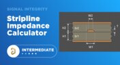
Stripline Impedance Calculator

Striplines provide some advantages over microstrips as they take advantage of natural shielding and coupling from nearby ground plane layers. Although they tend to experience higher losses due to total confinement in the dielectric, they can be thinner due to the high dielectric constant used in internal layers of a PCB. Use our free impedence calculator to help you determine the correct width needed to hit a target impedance.

Embedded thumbnail for Query Language: What is It For?
How-To's
Query Language: What is It For?

A PCB project contains many different objects. How to manage them? How to find the right ones quickly and efficiently? This video starts the series about query language. Learn the language commands and how to use them and expand your possibilities!

Blog
Which Types of Opto-Isolators Are Right For Your Signal?

An optoisolator is a cool electronic device that can be used to pass information between a diode without passing an electrical current. There are many great applications for these, but do you know which one is right for you?
Blog
Properties panel document options in SCH editors

The Properties panel provides access to the properties of documents and objects. The contents of the panel change depending on the active document or the selected object. This blog will quickly go over some of need to know options around the properties panel in the schematic document.

Embedded thumbnail for PCB design with BGA: Via-in-Pad
How-To's
PCB design with BGA: Via-in-Pad

We’ll teach you how to use Via-in-pad to reduce inductance, improve signal integrity, and improve power distribution system performance.

Embedded thumbnail for Design RF PCB: Distributed-Element Circuits
How-To's
Design RF PCB: Distributed-Element Circuits

Distributed-element circuits are a topology of a particular shape and size. Filters, power dividers, directional couplers can be built from them. Being calculated in third-party CAD, the topology of such elements can be easily imported into Altium Designer, and we will show you how to do it!

Embedded thumbnail for How to work with components on a rigid-flex board in MCAD
How-To's
How to work with components on a rigid-flex board in MCAD

With MCAD Codesigner you can quickly add and move components from your MCAD tool and update the design automatically in Altium Designer. We’ll show you how to. Add a new component, move components, and change a component’s region in MCAD, and update it to your design in Altium Designer.

Embedded thumbnail for LSM: Impedance profile
How-To's
LSM: Impedance profile

Creating Impedance profiles for transmission lines and how to apply them to the board

High-Speed PCB Stackup Design
Blog
The High-Speed PCB Stackup Design Challenge

Even with all the good guidelines out there for high speed design, there are particular aspects of stackup construction and their relation to building boards that get overlooked. This blog is goes beyond just the typical SI/PI guidelines and looks at these problems from more of an engineering perspective.

Embedded thumbnail for Multichannel Schematic: Creating Channels
How-To's
Multichannel Schematic: Creating Channels

Altium Designer makes creating single and multichannel designs effective and quick. We’ll show you how to create and annotate output and input channels in your design.

Embedded thumbnail for How to efficiently use Blankets?
How-To's
How to efficiently use Blankets?

Blanket is a powerful tool for group assignment of properties in schematic documents. It makes it easier and faster to assign circuit classes, differential pairs, and design rules within schematic documents. This video provides instructions on how to use blanket to simplify work in your designs.

stitching vias
Blog
Everything You Need to Know About Stitching Vias

Stitching vias are something you often see spread around the surface layer of a PCB, but what are they? and should you be using them? In this guide, we'll go over some of the standard uses of stitching vias and when they should be used in a PCB.

Embedded thumbnail for High Speed: XSignals for DDR3/DDR4
How-To's
High Speed: XSignals for DDR3/DDR4

In high speed design DDR3 and DDR4 memory chips can utilize xSignal classes to match track lengths from the controller to the memory chip easily and quickly. We’ll show you how using the xSignals wizard.

Embedded thumbnail for Design RF PCB: routing (any angle, arc)
How-To's
Design RF PCB: routing (any angle, arc)

It is worth taking a responsible approach to the shape and size of the RF signal conductors. In this video we will cover some practical aspects of working with routing such nets in Altium Designer.

PCB Stackup Basics
Blog
PCB Stackup Basics

In comparison to the build-up of a PCB, the stackup is more concerned with the electrical type of each layer, that is are we working with signals, power, or ground. Continue reading to learn how you can optimize your layer stack.

Embedded thumbnail for Draftsman Document: Snapping
How-To's
Draftsman Document: Snapping

Snapping using the grids and snapping tools in Altium Designer’s Draftsman Editor gives you a lot of control over how you create and annotate primitives and components. We’ll show you how easy it is to use snapping in the Drafstman Editor.

Embedded thumbnail for High Speed: XSignals
How-To's
High Speed: XSignals

You can create, configure, and utilize xSignals in Altium Designer to make your design process more efficient and effective. We’ll show you how to do it manually, using the more comprehensive Create xSignals command, and using the xSignal wizard.

Embedded thumbnail for DFM and fab cost/time constraints: What is annular ring and how to configure it
How-To's
DFM and fab cost/time constraints: What is annular ring and how to configure it

The minimum dimension from the wall of the aperture to the edge of the pad is called an annular ring, and we can configure it with Altium Designer. We’ll show you how to get started and manage the annular ring in your design rules.

Tag
Via current carrying capacity for PCBs
Blog
PCB Via Current-Carrying Capacity: How Hot is Too Hot?

One common question from designers is current-carrying capacity of conductors in a PCB. Trace and via current-carrying capacity are legitimate design points to focus on when designing a new board that will carry high current. The goal is to keep conductor temperatures below some appropriate limit, which then helps keep components on the board cool. Let’s dig into the current state of thermal demands on vias in PCBs and how they compare to internal and external PCB traces.

PCB Shield
Blog
Phalanx, not Failure: PCB Shielding to Protect Your Design

A combination of good printed circuit board design and good shielding mitigates EMI. Good PCB design for EMI shielding revolves around the layout, the placement of filters, and ground planes. A well-designed PCB minimizes parasitic capacitance and ground loops. Keep reading to learn more about PCB shielding.
Man working in Altium Designer
Blog
Best Practices in Hardware Version Control Systems

Any project can get very complex, and the PCB design team needs to track revisions throughout a project. Why worry about tracking revisions? In the event you ever receive changes to product functional requirements, major changes are made to your product’s architecture, or you’re ready to finalize the design and prepare for fabrication, it’s best to clone a project at its current state and begin working on a new version. Keeping track of all these design changes in a PCB design project takes the type of hardware version control tools you’ll find in Altium 365™.
Copper pour and via stitching
Blog
Copper Pour and Via Stitching: Do You Need Them in a PCB Layout?

To pour or not to pour, to stitch or not to stitch… Over many years, some common “rules of thumb” have become very popular and, ultimately, taken a bit out of context. Rules of thumb are not always wrong, but taking PCB design recommendations out of context helps justify bad design practices, and it can even affect the producibility of your board. Like many aspects of a physical PCB layout, via stitching and copper pour can be like acid: quite useful if implemented properly, but also dangerous if used indiscriminately.
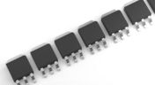
MOSFET Components
Blog
Should You Use Power MOSFETs in Series?

Power MOSFETs enable a huge range of electronic systems, specifically in situations where BJTs are not useful or efficient. MOSFETs can be used in high current systems in parallel arrangements, but what about their use in series? Both arrangements of MOSFETs have their pitfalls that designers should consider. Let’s look at MOSFETs in series as they are quite useful in certain systems, but be careful to design your circuits and your PCB for reliability.

MLCC controlled ESR capacitor
Blog
Controlled ESR Capacitors: Should You Use Them for Power Integrity?

I can’t think of a single product I’ve built that doesn’t require capacitors. We often talk a lot about effective series inductance (ESL) in capacitors and its effects on power integrity. What about effective series resistance (ESR)? Is there a technique you can use to determine the appropriate level of resistance, and can you use ESR to your advantage?
Ground Pour, Impedance and Losses
Blog
Microstrip Ground Clearance Part 2: How Clearance Affects Losses

If your goal is to hit a target impedance, and you’re worried about how nearby pour might affect impedance, you can get closer than the limits set by the 3W rule. But what are the effects on losses? If the reason for this question isn’t obvious, or if you’re not up-to-date on the finer points of transmission line design, then keep reading to see how nearby ground pour can affect losses in impedance-controlled interconnects.
Choosing the Right Microphone for Embedded Applications
Blog
Choosing the Right Microphone for Embedded Applications

If you need to capture sound waves for your electrical device to process, you'll need a microphone. However, microphones these days have become very advanced, and there are so many options to choose from. They range from the relatively simple and popular condenser type microphones to state-of-the-art sound conversion solutions incorporating internal amplifiers and other electronic processing functionality. In this article, we'll take a look at some of the options available.
 Computer planet with circuit grid
Blog
Composite Amplifiers and How They Give the Best of Both Worlds

There are many times where you need an amplifier with high gain, low noise, high slew rate, and broad bandwidth simultaneously. However, not all of these design goals are possible with all off-the-shelf components. Here are some points to consider when working with a composite amplifier design and how to evaluate your design with the right set of circuit simulation tools.
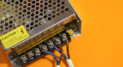
Impedance balancing power supply
Blog
Reduce Common-Mode Noise in Your Power Supply with Impedance Balancing

Simple switching regulator circuits that operate in compact spaces, like on a small PCB, can usually be deployed in noisy environments without superimposing significant noise on the output power level. As long as you lay out the board properly, you’ll probably only need a simple filter circuit to remove EMI on the inputs and outputs. As the regulator becomes larger, both physically and electrically, noise problems can become much more apparent, namely radiated EMI and conducted EMI in the PCB layout.
Part 1: Why Your PCB Design Review Process Is Obsolete and What You Can Do About It
Blog
Part 1: Why Your PCB Design Review Process Is Obsolete and What You Can Do About It

A PCB design review is a practice to review the design of a board for possible errors and issues at various stages of product development. It can range from a formal checklist with official sign-offs to a more free-form inspection of schematic drawings and PCB layouts. For this article, we will not delve into what to check during a design review process but rather look at how a review process itself usually unfolds and how to optimize it to get the most out of your time.
Star ground PCB
Blog
What is PCB Star Grounding and Why Would Anyone Use It?

If you look on the internet, you'll find some interesting grounding recommendations, and sometimes terminology gets thrown around and applied to a PCB without the proper context or understanding of real electrical behavior. DC recommendations get applied to AC, low current gets applied to high current, and vice versa... the list goes on. One of the more interesting grounding techniques you'll see as a recommendation, including on some popular engineering blogs within the industry, is the use of PCB star grounding.
Silkscreen on PCB
Blog
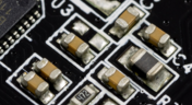
Your Guide to PCB Silkscreen

Every PCB has silkscreen on the surface layer, and you’ll see a range of alphanumeric codes, numbers, markings, and logos on PCB silkscreen. What exactly does it all mean, and what specifically should you include in your silkscreen layer? All designs are different, but there are some common pieces of information that will appear in any silkscreen in order to aid assembly, testing, debug, and traceability
Gibbs ringing
Blog
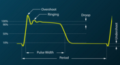
What Causes Gibbs Ringing in High-speed Channel Simulations?

Designing high-speed channels on complex boards requires simulations, measurements on test boards, or both to ensure the design operates as you intend. Gibbs ringing is one of these effects that can occur when calculating a channel’s response using band-limited network parameters. Just as is the case in measurements, Gibbs ringing can occur in channel simulations due to the fact that network parameters are typically band-limited.
Heated component on PCB
Blog
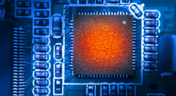
Efficient Heat Dissipation with SMD Heat Sinks Keeps You From Dropping PCBs

In electronics, there is the possibility that your PCB can get pretty hot due to power dissipation in certain components. There are many things to consider when dealing with heat in your board, and it starts with determining power dissipation in your design during schematic capture. If you happen to be operating within safe limits in a high power device, you might need an SMD heat sink on certain components. Ultimately, this could save your components, your product, and even the operator.


Tag
NEW
Embedded thumbnail for Coming Soon: Advanced Via Fencing
New in Altium's Software
Coming Soon: Advanced Via Fencing

Coming soon to Altium software: Advanced Via Fencing gives you greater control over creating and managing shielding and stitching vias for RF and high-speed designs. Configure via fences directly from the Properties panel, follow traces or geometry edges, use stacked vias, define spacing and patterns, and preview the results before generating them.

NEW
Embedded thumbnail for 5 DC Power Integrity Myths That Ruin Your PCB Design
How-To's
5 DC Power Integrity Myths That Ruin Your PCB Design

DC power integrity plays a critical role in the reliability of nearly every power electronics board, yet common misconceptions can lead to costly design decisions. In this video, we break down five of the most common DC power integrity myths and explain what you really need to know for reliable power electronics design.

Embedded thumbnail for A fraction of a millimeter is the difference between a robot that fits and one that doesn't
Collaborative Engineering with Team Ribbot
A fraction of a millimeter is the difference between a robot that fits and one that doesn't

Check out the latest episode about Team Ribbot and see how they move design data between their electrical and mechanical tools without losing accuracy. Discover how Altium Designer and MCAD CoDesign help bring the boards, housings, and custom motors together right the first time with no surprises.

Embedded thumbnail for  HDI PCB Stackup Breakdown - Etching Weight Via Spacing, & More
How-To's
HDI PCB Stackup Breakdown - Etching Weight Via Spacing, & More

HDI PCB design depends on getting the stackup and manufacturing constraints right. In this deep dive, we examine a real HDI audio-interface board and explore common pitfalls, from how copper weight and etching affect minimum clearances to why solder mask slivers below 1 mil can cause manufacturing issues. You’ll also learn how proper board-edge clearance and copper pullback help protect SMD pads during routing.

Embedded thumbnail for  How do you review a robot design when your team is never in the same room?
Collaborative Engineering with Team Ribbot
How do you review a robot design when your team is never in the same room?

Team Ribbot’s engineers are spread across five states and juggle full-time jobs while building a 250-pound combat robot in their spare time. Discover how Altium Designer and Altium 365 keep the team connected, letting engineers open the live design from a laptop or phone, inspect the board in 3D, and leave comments directly on the design.

Embedded thumbnail for  Improve Visual Accuracy with True Arcs
New in Altium's Software
Improve Visual Accuracy with True Arcs

Discover how True Arc Rendering improves arc visualization in the PCB Editor and PCB Library Editor by displaying true arcs across 2D, 3D, and Board Planning modes. This provides a more accurate representation of board geometry and helps you work with curved features with greater precision throughout the design process.

Embedded thumbnail for Two engineers, one board, nobody's work gets wiped out
Collaborative Engineering with Team Ribbot
Two engineers, one board, nobody's work gets wiped out

When Team Ribbot’s electrical and mechanical engineers work on the same combat-robot design, unwanted changes can mean hours of lost work. See how Altium Designer and MCAD CoDesign let the team review and selectively accept changes, enabling seamless parallel collaboration across different locations and schedules.

Embedded thumbnail for Visualize and Refine Your Harness Designs
New in Altium's Software
Visualize and Refine Your Harness Designs

Create detailed views of bundle contents, control wire and cable paths, and rotate physical models to accurately represent the final harness assembly. These capabilities give you greater control over harness design and help ensure your digital model reflects the physical result.

Embedded thumbnail for Introducing Agentic Requirements Engineering
New in Altium's Software
Introducing Agentic Requirements Engineering

Discover a new way to work with Requirements Portal through Agentic Requirements Engineering. AI agents analyze your project data and surface proposals for your approval, reducing friction in requirements management and helping align your team's shared model with your design intent.

Embedded thumbnail for Simplify Rule Set Updates and Replacement
New in Altium's Software
Simplify Rule Set Updates and Replacement

Learn how to import rule sets with greater flexibility in Altium. When importing rules, you can add new rules to your existing set, replace only rules that match, or completely replace the current rule set giving you full control over how design rules are updated.

Embedded thumbnail for  How Team Ribbot fits 40 kW of power into a 250-pound combat robot
Collaborative Engineering with Team Ribbot
How Team Ribbot fits 40 kW of power into a 250-pound combat robot

What do you get when you pack the power of a small electric car into a combat robot with virtually no room to spare? In the first episode of our collaboration with Team Ribbot and Altium, explore how seamless ECAD-MCAD collaboration helps the team tackle complex design challenges, optimize high-performance designs, reduce errors, and bring products to life faster.

Embedded thumbnail for Just Released: Supplier Data Merging
New in Altium's Software
Just Released: Supplier Data Merging

Discover how the Supplier Data Merging feature brings together supplier information from your custom parts database and the Altium Parts Provider into a single, unified view. Access consolidated supplier data wherever supplier part numbers appear, including in ActiveBOM and during component selection.

Embedded thumbnail for How Altium’s Layer Stack Manager Actually Works
How-To's
How Altium’s Layer Stack Manager Actually Works

Take a look inside Altium's Layer Stack Manager and discover how its impedance calculator determines the ideal trace width for your target impedance. In this video, we break down the "black box" behind the calculation and show how the Simbeor-based field solver provides accurate results while eliminating the need for advanced field solver expertise.

Embedded thumbnail for Connect Requirements Directly to Your PCB Design
New in Altium's Software
Connect Requirements Directly to Your PCB Design

See how the Requirements Portal integration in Altium Designer simplifies requirements management by bringing system requirements directly into your PCB design workflow. Connect requirements to design documents, assign tasks, track verification in real time, and keep your entire team aligned with seamless synchronization in Altium 365.

Embedded thumbnail for SFP Connector Routing: High-Speed Differential Pair Design Tips
How-To's
SFP Connector Routing: High-Speed Differential Pair Design Tips

Discover practical SFP and SFP+ routing tips in our latest video, inspired by a real question from the Altium subreddit. We cover how aggressive serpentine length tuning can be, how to reduce impedance discontinuities in tight meanders, and how meandering influences mode conversion at 10G and higher data rates.

Embedded thumbnail for Handle High-Density PCB Layouts with Ease
New in Altium's Software
Handle High-Density PCB Layouts with Ease

Push the limits of PCB design with support for up to 128 signal layers, empowering the development of even the most complex, high-density boards.

Tag
Your search returns no results.