
Main navigation

  • Home
  • Discover
  • Learning Center
  • What’s New

Second main navigation

  • Altium Community
  • Support
  • Documentation
×

Results

  • Updates
  • Blog 570
  • Video 539
  • Webinar 86
  • Playlist 53
Filters:
Tag (field_common_tag)
Blog • May 12, 2025
Printed Electronics: The Future of Flexible and Cost-Effective Circuit Design

This article explores the rise of printed electronics as a lightweight, flexible, and cost-effective alternative to traditional PCB design. It highlights key benefits like reduced manufacturing costs, sustainability, and new design possibilities—especially in wearables, medical devices, and automotive applications. 

Read More
Embedded thumbnail for Unveiling 86% Task Time Efficiency in Altium Designer 25
Altium Designer's 25 Quantitative Benefits • May 9, 2025
Unveiling 86% Task Time Efficiency in Altium Designer 25

Watch how Altium Designer 25 saves time on PCB visualization. This short video shows a side-by-side comparison of the same task done in Altium Designer 25 vs. an external CAD tool—revealing big time and click savings. A great teaser to highlight the value of the unified design environment and promote the Benefit Calculator.

Start Watching
Embedded thumbnail for AGND vs PGND: Proper Net Tie Connections in Power Regulator PCB Design
How-To's • May 8, 2025
AGND vs PGND: Proper Net Tie Connections in Power Regulator PCB Design

What’s the difference between AGND and PGND — and when should you use a net tie? Zach Peterson breaks down proper PCB layout for buck converters, grounding best practices, and why component placement matters in switching regulator designs.

Start Watching
Blog • May 7, 2025
How to Choose the Best Requirements Management Tool for Electronics Development

Many electronics teams still rely on documents and spreadsheets for requirements management—leading to gaps, errors, and delays. Alexsander Tamari explores better tools to improve traceability, collaboration, and project outcomes.

Read More
Blog • May 6, 2025
New Routing Possibilities with Ultra HDI

Explore how Ultra HDI technology is redefining PCB design. This article breaks down the benefits and manufacturing considerations of Ultra HDI, and how it enables next-level routing density and miniaturization in advanced electronics.

Read More
Blog • May 5, 2025
3D-MID in Focus: Principles, Processes, and Practical Use

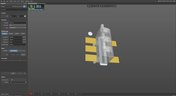
This article introduces 3D-MID (Mechatronic Integrated Devices), a technology that integrates circuitry into 3D plastic structures to reduce size, weight, and complexity. It explains the production process, use cases, and benefits of 3D-MID in sectors like automotive, medical, and consumer electronics.

Read More
Embedded thumbnail for  Students at Monash UAS Fly Higher with Altium Solutions to Power Their Autonomous Drone Technology
Altium Stories • May 2, 2025
Students at Monash UAS Fly Higher with Altium Solutions to Power Their Autonomous Drone Technology

Discover how the Monash Uncrewed Aerial Systems team leverages Altium Designer, MCAD CoDesigner, and Altium 365 to develop custom drone boards for critical humanitarian missions.

Start Watching
Blog • Apr 30, 2025
Eliminate EMI and Signal Integrity Issues in Multi-Board PCB Designs

Ensure signal integrity and minimize EMI in complex electronics. Our new article explains how to address electromagnetic interference and signal integrity challenges in multi-board PCB designs, offering practical strategies and layout considerations for reliable system performance.

Read More
Embedded thumbnail for Say Goodbye to Disjointed Workflows: Unified Product Design in Altium Designer 25
New in Altium Designer 25 • Apr 29, 2025
Say Goodbye to Disjointed Workflows: Unified Product Design in Altium Designer 25

Check an overview of how Altium Designer 25 unifies Multi-Board and Harness Design into a seamless, efficient workflow for faster, error-free product development.

Start Watching
Embedded thumbnail for From Concept to Reality: Updated 3D-MID Demo in Altium Designer 25
New in Altium Designer 25 • Apr 28, 2025
From Concept to Reality: Updated 3D-MID Demo in Altium Designer 25

A walkthrough of the new 3D-MID capabilities in Altium Designer 25. Covers setting up a 3D PCB document, component placement on curved surfaces, routing with grids and sketches, exporting for LDS manufacturing, and generating a 3D pick-and-place file.

Start Watching
Blog • Apr 25, 2025
How to Overcome Power Distribution and Connector Misalignment Challenges in Multi-Board PCB Systems

Connector misalignment can compromise the reliability of power delivery in multi-board systems. This article explores the causes, effects, and prevention strategies for connector misalignment in power distribution, helping you design more robust multi-board PCB systems.

Read More
Embedded thumbnail for Take 66% of Your Time Back with Custom Pad Stack in Altium Designer 25
Altium Designer's 25 Quantitative Benefits • Apr 24, 2025
Take 66% of Your Time Back with Custom Pad Stack in Altium Designer 25

This video demonstrates the measurable productivity gains of using the Custom Pad Stack tool in Altium Designer 25. It compares a detailed QFN-32 footprint customization process across versions, showing a significant reduction in time and mouse clicks—2 min 5 sec vs. 6 min 2 sec, and 45 vs. 116 clicks.

Start Watching
Blog • Apr 22, 2025
Mastering Component Templates in Altium Designer 25

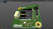
Our new article by Dario Fresu explains how Component Templates in Altium Designer 25 Pro improve design consistency, reduce errors, and streamline collaboration. It highlights practical benefits like standardized naming, faster component creation, and scalability across projects. Includes examples of using templates with Altium 365™ to simplify complex component setup.

Read More
Embedded thumbnail for PCB Stackups in Reverse?
How-To's • Apr 21, 2025
PCB Stackups in Reverse?

Watch our new tutorial on reverse PCB stackups — a unique approach that combines thin internal layers with thicker outer cores for specialized applications. Learn how to implement reverse stackups effectively in Altium Designer, understand key manufacturability constraints, and explore Rogers materials specifically suited for this technique.

Start Watching
Blog • Apr 18, 2025
Wire Harness Design Guide for Development and Manufacturing

Designing a wire harness goes far beyond just connecting components—it’s about ensuring manufacturability, reliability, and compliance. This article walks you through the entire process, from initial design to production, helping you streamline development and avoid common pitfalls.

Read More
Embedded thumbnail for Design Smarter - Harness, Multi-board, and MCAD CoDesign in Action
New in Altium Designer 25 • Apr 16, 2025
Design Smarter - Harness, Multi-board, and MCAD CoDesign in Action

This webinar highlights how Altium Designer 25, with a Pro or Enterprise subscription, enables seamless ECAD-MCAD collaboration using Harness and Multi-board Design tools and the advanced MCAD CoDesigner. Viewers will learn how to integrate harness designs, optimize multi-board systems for enclosure fit, and synchronize designs with SolidWorks, PTC Creo, and Autodesk Inventor.

Start Watching
  • Show More
Tag (field_common_tag)
Blog • Jul 2, 2025
PCB First-Pass Yield: Small Decisions That Make a Big Difference

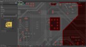
This article highlights how seemingly minor layout choices like trace spacing, component footprints, or stack-up details can dramatically impact whether a board passes fabrication and assembly the first time.

Read More
Blog • Jul 1, 2025
Implementing Design for Supply Chain Principles in Electronic Product Development

Designing with supply chain principles in mind helps you avoid delays, reduce costs, and ensure manufacturability. This article outlines practical strategies for component selection, sourcing, and lifecycle management to make your designs more resilient and production-ready.

Read More
Blog • Jun 27, 2025
Beyond the BOM: How Proactive Component Selection Is Transforming Workflows

Learn how proactive component selection helps you avoid supply chain risks, reduce costs, and design more reliably. Our new article outlines key strategies and shows how tools like Altium 365 support smarter part decisions.

Read More
Blog • Jun 26, 2025
Power Integrity Issues?

Power problems can be hard to spot until it’s too late. See how easy it is to analyze your power nets, check voltage drops, and improve reliability with Power Analyzer by Keysight - all without leaving your design environment.

Read More
Blog • Jun 24, 2025
How to Design High-Speed PCBs Without Signal Surprises

Signal issues can sneak in early and cost you later. Read our whitepaper to see how Signal Analyzer by Keysight (inside Altium Designer) helps you catch problems fast and design with confidence.

Read More
Blog • Jun 18, 2025
Beyond Basic Part Selection: Using Supply Chain Data to Validate Choices

Learn how to enhance part selection by using real-time supply chain data. This article shows how integrating insights like availability and lifecycle status helps you make smarter, risk-aware design choices.

Read More
Blog • Jun 17, 2025
Signal Mistakes Are Expensive

See how the Signal Analyzer by Keysight in Altium Designer lets you run signal integrity checks directly within your design environment. Read our article to learn how to effectively manage impedance, return paths, stackups, and more.

Read More
Blog • Jun 12, 2025
Twice the Insight. One Seamless Simulation Bundle

Ensure power and signal integrity with the Keysight Bundle in Altium Designer. Catch issues early, reduce rework, and optimize your PCBs - all within one integrated environment featuring Signal & Power Analyzer.

Read More
Blog • Jun 3, 2025
Preparing for Prototype: Final Component Validation

Final component validation is the last critical check before building a prototype, ensuring all parts are accurate, available, and viable. This article shows how Altium’s integrated tools—like SiliconExpert, Z2Data, Octopart, and BOM Portal—help teams avoid costly surprises and prepare with confidence.

Read More
Blog • Jun 2, 2025
Getting Started with Harness Design in Altium Designer 25

Explore the essential steps and tools for Harness Design in Altium Designer 25, from initial setup to final documentation. The article highlights how the unified design environment streamlines the entire process, improving efficiency and project integration.

Read More
Blog • May 30, 2025
The Future of PCB Design Starts Here

Altium Designer is constantly evolving, with powerful new features and updates on the way. Get an exclusive first look at what’s coming next—visit our Coming Soon page to stay up to date with the latest innovations.

Read More
Blog • May 29, 2025
Simplify Harness-to-System Connections for Better PCB Design Outcomes

Struggling to keep harness and system designs in sync? In our brand-new article we explore how integrating PCB and harness design workflows can eliminate errors, improve collaboration, and accelerate your development process. Discover a smarter approach to connecting your harness to the system.

Read More
Blog • May 27, 2025
The Crucial Balance: Cost, Quality, and Availability In Electronic Component Selection

Balancing cost, quality, and availability is key when selecting electronic components. This article explores how to make informed choices that meet design goals while managing supply chain and sourcing challenges.

Read More
Blog • May 19, 2025
Wire Harness Failures: The Hidden Costs and Real-World Recalls That Could Have Been Prevented

Wire harness failures can lead to significant financial losses, production delays, and safety hazards. This article delves into real-world examples of such failures across industries and illustrates how modern CAD tools can help prevent these costly issues.

Read More
Blog • May 13, 2025
Part Selection Fundamentals: Creating Resilient Component Requirements

Learn how to ensure electronic components meet the demands of harsh environments. This article explores key standards, testing protocols, and design considerations for building resilient systems that perform reliably under extreme conditions.

Read More
Blog • May 12, 2025
Printed Electronics: The Future of Flexible and Cost-Effective Circuit Design

This article explores the rise of printed electronics as a lightweight, flexible, and cost-effective alternative to traditional PCB design. It highlights key benefits like reduced manufacturing costs, sustainability, and new design possibilities—especially in wearables, medical devices, and automotive applications. 

Read More
  • Show More
Tag (field_common_tag)
Embedded thumbnail for How to Improve Routing Using Glossing
How-To's • Jul 14, 2021
How to Improve Routing Using Glossing

Routes for your design can get messy, leading to inefficiency and waste. Altium Designer’s Glossing features can help! We’ll show you how to clean up your interactive routing as you route, how to gloss tracks already routed, and some tips and tricks to clean them up exactly how you want them.

Start Watching
Embedded thumbnail for Tenting Vias in Altium Designer
How-To's • Jul 12, 2021
Tenting Vias in Altium Designer

This video shows how to tent vias in Altium Designer by using design rules. Since vias are often located very close to pads, during assembly, solder paste sometimes flows into vias, which, in turn, leads to poor soldering quality. To avoid this, cover vias with a solder mask layer.

Start Watching
Embedded thumbnail for How to Create and Validate Return Paths in Altium Designer
How-To's • Jul 9, 2021
How to Create and Validate Return Paths in Altium Designer

For high-speed projects where there are lines with a given impedance, it is important to maintain a consistent return signal path. For the return signal, reference planes are created in the form of polygons and the polygons must maintain integrity along the entire path of the signal. This video shows how consistent return paths are created and validated. 

Start Watching
Embedded thumbnail for How to Edit Component Directly on PCB
How-To's • Jul 5, 2021
How to Edit Component Directly on PCB

Once you’ve pulled your components with an ECO into the PCB you may need to edit them. We’ll show you how to edit your components in the PCB view.

Start Watching
Embedded thumbnail for How to Control Tuning in Altium Designer
How-To's • Jul 1, 2021
How to Control Tuning in Altium Designer

When dealing with high frequency boards, it is necessary to match the timing of certain nets and differential pairs. In this video, we’ll go over how to use the tuning tool to match trace lengths based on the design rules. Using the Interactive Length Tuning command, you will begin tuning and can then use the Properties panel to configure the properites of the tuning segment.

Start Watching
Embedded thumbnail for How to Use Text Justification
How-To's • Jun 30, 2021
How to Use Text Justification

This video demonstrates how to use the justification function to align text on the PCB.

Start Watching
Embedded thumbnail for How to control net propagation delay
How-To's • Jun 16, 2021
How to control net propagation delay

When dealing with high-frequency boards it's necessary to match the timing of certain nets and differential pairs. In this video, we’ll go over how to use the tuning tool to match trace lengths based on design rules. 

Start Watching
Embedded thumbnail for How to Edit or Manage Board Shape
How-To's • Apr 23, 2021
How to Edit or Manage Board Shape

Board shapes can be edited and managed several different ways in Altium Designer. We’ll show you how using 2D and 3D modes and models as well as importing from DXF or DWG.

Start Watching
Embedded thumbnail for How to define The Impedance Profile For a Coplanar Stripline
How to Work with Differential Pairs • Apr 16, 2021
How to define The Impedance Profile For a Coplanar Stripline

In this video, we show how to determine the impedance of a coplanar stripline. The impedance is configured on the Impedance tab of the Layer Stack Manager. When calculating the impedance, the Layer Stack Manager takes into account the material parameters and the distance to the return conductors.

Start Watching
Embedded thumbnail for How to Create Complex Keepout Shapes
How-To's • Apr 9, 2021
How to Create Complex Keepout Shapes

Keepout regions are easy to create in Altium Designer, but they can be complex. We’ll show you a few ways to make creating your more complex keepout shapes easier and more efficient.

Start Watching
Embedded thumbnail for How to Use a Courtyard Layer for the Component Boundary
How-To's • Apr 2, 2021
How to Use a Courtyard Layer for the Component Boundary

In this video, you will see how to use the courtyard layer as a component boundary.

Start Watching
Embedded thumbnail for Creating High-speed Signal Classes with xSignals
How To Work with High-Speed Projects • Feb 8, 2021
Creating High-speed Signal Classes with xSignals

You can create, configure, and utilize xSignals in Altium Designer to make your design process more efficient and effective. We’ll show you how to do it manually, using the more comprehensive Create xSignals command, and using the xSignal wizard.

Start Watching
Embedded thumbnail for New Shortkeys for Better 3D Scene Control
New in Altium Designer 21 • Dec 28, 2020
New Shortkeys for Better 3D Scene Control

One of the hallmarks of Altium Designer is the visualization and 3D tools. With each version, more features and tools appear. Altium Designer 21 is no exception, and one of the improvements in 3D mode is the appearance of a rotation button in the properties of models, with the help of which the 3D model is rotated 90 degrees along the corresponding axis. And the arrows on the additional keyboard that correspond to the numbers 2, 4, 6, 8 are hot buttons for quickly rotating the model along the axes. Thus, providing the ability to quickly position any 3D model in the desired plane.

Start Watching
Embedded thumbnail for Embedded Board Arrays at Any Angle
New in Altium Designer 21 • Dec 28, 2020
Embedded Board Arrays at Any Angle

An embedded board array is a primitive design object. It allows you to create a PCB panel as part of your PCB design project. This is also known as panelization. In the new version of AD21, Embedded board arrays can now be placed at any angle within a PCB fabrication panel, which offers improved flexibility in how unusually shaped PCBs in particular can be arranged to maximize the available board panel real-estate.

Start Watching
Embedded thumbnail for Insert Logo or Any Images on PCB
New in Altium Designer 21 • Dec 28, 2020
Insert Logo or Any Images on PCB

In the process of designing a printed circuit board, it becomes necessary to apply additional marking. It can be a company logo, interface designation or additional information signs. For ease of creating additional markings in Altium Designer 21, the PCB editor has a new Graphics tool that allows you to insert a picture into a specified area. This tool supports any of the four formats JPG, BMP, PNG, SVG. After selecting the image, it remains to specify its quality and the tool converts the image into a region on the active layer. If necessary, you can invert the image.

Start Watching
Embedded thumbnail for Using Polygons on Power Planes
New in Altium Designer 21 • Dec 28, 2020
Using Polygons on Power Planes

Traditionally, a PCB power plane is designed as a negative, that is, the objects placed on a power plane layer become voids in the copper when the board is fabricated. This approach is used because it is more efficient to generate the output data this way, as the bulk of a plane layer is normally copper; voids in the copper are only needed in specific locations such as around non-connected pads, or as separation voids when the plane is divided into different voltage regions.

Start Watching
  • Show More
Tag (field_common_tag)
Altium Enterprise
On-Demand Webinar • May 10, 2025
Streamline your customer relation with Altium 365 Enterprise
Join our webinar designed for engineers and users in EMS companies
Watch Now
PCB
On-Demand Webinar • May 1, 2025
Altium Designer Overview
Altium Designer is the #1 PCB design tool for a reason. Join us for this live webinar and get an inside look at Altium’s world-class PCB design solution. See for yourself why design teams around the globe are making the switch to Altium Designer. Register now!
Watch Now
Enterprise
On-Demand Webinar • Apr 25, 2025
Altium Customization with Scripting or Low-Code
See how scripting, low-code, no-code, and API integrations can help you work more efficiently—without extra setup or complex systems.
Watch Now
A365 Webinar: Altium BOM Portal - From PCB Design to Parts Ordering in Minutes
On-Demand Webinar • Apr 21, 2025
Altium 365 BOM Portal - From PCB Design to Parts Ordering in Minutes
Join us to learn how to reduce sourcing time by up to 70% using Altium 365 BOM Portal.
Watch Now
April 2025 COM Webinar
On-Demand Webinar • Apr 17, 2025
Advanced xSignal and Impedance Control Techniques
We are hosting a free webinar on advanced xSignal configuration and impedance control techniques in Altium Designer to help you tackle signal integrity challenges. Register now to enhance your design skills.
Watch Now
Altium Enterprise
On-Demand Webinar • Mar 25, 2025
Unlocking the full potential of your design team with Altium's enterprise solution
See how Altium's enterprise solution can help you meet your electronic product design goals
Watch Now
Transmission line
On-Demand Webinar • Mar 4, 2025
Optimizing Layer Stackup and Impedance for High-Speed PCB Design
Learn how to master the layer stack manager to efficiently create stackups, manage materials, and ensure optimal design performance.
Watch Now
Harness design
On-Demand Webinar • Mar 2, 2025
Design Smarter - Harness, Multi-board, and MCAD CoDesign in Action
Discover how the latest Harness, Multi-board, and MCAD CoDesign tools can revolutionize your PCB design workflow.
Watch Now
ADv25
On-Demand Webinar • Jan 30, 2025
6 Reasons to Switch Design Tools
Come see how Altium Designer, the industry standard for PCB design, combined with Altium 365 delivers the world’s first connected PCB design experience.
Watch Now
PCB CoDesign
On-Demand Webinar • Jan 29, 2025
Level Up Your Team's Productivity with Altium
Discover how to create an efficient, collaborative, and transparent design process for your team!
Watch Now
Assembly variants
On-Demand Webinar • Jan 9, 2025
Designing with Assembly Variants
Join us to learn best practices and get into the details about setting up variants in your designs and speeding up your project development.
Watch Now
Single layer PCB
On-Demand Webinar • Jan 8, 2025
Optimized for Success - Advanced PCB Features in Altium Designer
This webinar will show you how to use the latest PCB Layout, signal integrity analysis, and component management design tools in Altium Designer.
Watch Now
Rigid flex
On-Demand Webinar • Dec 19, 2024
How To Use Modern Rigid-Flex Substrates
Join us in this webinar where we’ll go over how you can easily create your own flex design.
Watch Now
Power Analyzer
On-Demand Webinar • Oct 29, 2024
Power Integrity Made Simple
Power Analyzer by Keysight in Altium Designer makes it easy to resolve PDN issues that arise during the board design process within a unified design environment.
Watch Now
Electronic Component Traceability
On-Demand Webinar • Oct 25, 2024
Ensuring Electronic Component Traceability From Idea to Innovation
Watch the webinar to learn how to achieve full transparency, improve collaboration, and ensure compliance throughout your entire supply chain—whether you are sourcing domestically or abroad.
Watch Now
Why Altium Designer is Your Next Step for PCB Design
On-Demand Webinar • Oct 24, 2024
Why Altium Designer is Your Next Step for PCB Design
Join us to see how moving to Altium Designer can enable resilient and scalable designs while streamlining your entire workflow.
Watch Now
  • Show More
Tag (field_common_tag)
Loading
Loading...
Share link
Share with
Search by Update
Version
Update
25 26 24 23 22
25.0 25.1 25.2 25.3 25.4 25.5 25.6 25.7 25.8 25.9
26.1 26.2
24.10 24.9 24.8 24.7 24.6 24.5 24.4 24.3 24.2 24.1 24.0
23.11 23.10 23.9 23.8 23.7 23.6 23.5 23.4 23.3 23.2 23.1 23.0
22.11 22.10 22.9 22.8 22.7 22.6 22.5 22.4 22.3