
Main navigation

  • Home
  • Discover
  • Learning Center
  • What’s New

Second main navigation

  • Altium Community
  • Support
  • Documentation
×

Results

  • Updates
  • Blog 570
  • Video 539
  • Webinar 86
  • Playlist 53
Filters:
Tag (field_common_tag)
Embedded thumbnail for Enhanced Constraint Manager in Altium Designer 25. Part I: From Directives to Creepage Rules
Enhanced Constraint Manager in Altium Designer 25 • Jun 9, 2025
Enhanced Constraint Manager in Altium Designer 25. Part I: From Directives to Creepage Rules

We are introducing a new video series on the Enhanced Constraint Manager in Altium Designer 25. In the first chapter, Samer Aldhaher demonstrates how to define net classes, apply clearance and creepage rules, and validate constraints within both the schematic and PCB. The video uses a 1kW, 400V brushless DC motor driver project to illustrate real-world applications.

Start Watching
Embedded thumbnail for Design Faster with Altium Designer 25
Altium Designer's 25 Quantitative Benefits • Jun 6, 2025
Design Faster with Altium Designer 25

Every second and every click count in the product development cycle. See how the new PCB Layout Replication feature in Altium Designer 25 boosts your efficiency in the PCB design process. Want to improve even more? Check out our Benefit Calculator now!

Start Watching
Embedded thumbnail for Creating PCB Drill Drawings and Tables in Altium Designer
How-To's • Jun 5, 2025
Creating PCB Drill Drawings and Tables in Altium Designer

If you want to learn more about drill drawings and tables in your PCB designs using Altium Designer, this tutorial is a must-watch. In the video, our Tech Consultant Zach Peterson walks you through multiple methods for generating these critical fabrication documents, including automatic Gerber outputs and custom drawings.

Start Watching
Embedded thumbnail for Streamlining Team Collaboration in Industrial PCB Projects - Recording Preview
New in Altium Designer 25 • Jun 4, 2025
Streamlining Team Collaboration in Industrial PCB Projects - Recording Preview

This webinar recording shows how Altium Designer and Altium 365 improve team collaboration in industrial PCB projects. It covers features like version control, live commenting, task tracking, and JIRA integration to help teams work more efficiently and reduce costly errors.

Start Watching
Blog • Jun 3, 2025
Preparing for Prototype: Final Component Validation

Final component validation is the last critical check before building a prototype, ensuring all parts are accurate, available, and viable. This article shows how Altium’s integrated tools—like SiliconExpert, Z2Data, Octopart, and BOM Portal—help teams avoid costly surprises and prepare with confidence.

Read More
Blog • Jun 2, 2025
Getting Started with Harness Design in Altium Designer 25

Explore the essential steps and tools for Harness Design in Altium Designer 25, from initial setup to final documentation. The article highlights how the unified design environment streamlines the entire process, improving efficiency and project integration.

Read More
Blog • May 30, 2025
The Future of PCB Design Starts Here

Altium Designer is constantly evolving, with powerful new features and updates on the way. Get an exclusive first look at what’s coming next—visit our Coming Soon page to stay up to date with the latest innovations.

Read More
Blog • May 29, 2025
Simplify Harness-to-System Connections for Better PCB Design Outcomes

Struggling to keep harness and system designs in sync? In our brand-new article we explore how integrating PCB and harness design workflows can eliminate errors, improve collaboration, and accelerate your development process. Discover a smarter approach to connecting your harness to the system.

Read More
Embedded thumbnail for AC Coupling Capacitors: Placement for High-Speed PCB Design
How-To's • May 28, 2025
AC Coupling Capacitors: Placement for High-Speed PCB Design

Learn the facts about AC coupling capacitor placement in high-speed PCB designs. In this video, Zach Peterson explores the ongoing debate: should AC coupling capacitors be placed near the transmitter or the receiver in high-speed differential pairs?

Start Watching
Blog • May 27, 2025
The Crucial Balance: Cost, Quality, and Availability In Electronic Component Selection

Balancing cost, quality, and availability is key when selecting electronic components. This article explores how to make informed choices that meet design goals while managing supply chain and sourcing challenges.

Read More
Embedded thumbnail for Coming Soon: Export 3D-MID Tracks as Centerline Curves
New in Altium Designer 25 • May 23, 2025
Coming Soon: Export 3D-MID Tracks as Centerline Curves

Coming Soon: 3D-MID Track-to-Centerline Export allows you to export conductive tracks on 3D substrates as precise centerline curves within STEP files—enabling seamless integration with advanced 5-axis manufacturing processes. Explore more upcoming upgrades on our Coming Soon page.

Start Watching
Embedded thumbnail for Advanced xSignal and Impedance Control Techniques - Recording Preview
New in Altium Designer 25 • May 20, 2025
Advanced xSignal and Impedance Control Techniques - Recording Preview

This webinar recording explores advanced xSignal and impedance control techniques in Altium Designer 25. It covers defining xSignals, managing impedance profiles, differential pairs, and delay tuning—all essential for high-speed PCB design. Full recording you find here: April 2025 COM Webinar Recording.

Start Watching
Blog • May 19, 2025
Wire Harness Failures: The Hidden Costs and Real-World Recalls That Could Have Been Prevented

Wire harness failures can lead to significant financial losses, production delays, and safety hazards. This article delves into real-world examples of such failures across industries and illustrates how modern CAD tools can help prevent these costly issues.

Read More
Embedded thumbnail for Coming Soon: Embedded 3D Models for Harness Designs
How-To's • May 16, 2025
Coming Soon: Embedded 3D Models for Harness Designs

Coming soon: the Embedded 3D Models for Harness Designs feature will automatically include Parasolid-format 3D models in your harness layout drawings. This improves integration with MCAD CoDesigner, enabling seamless synchronization between electrical and mechanical design domains. To see more upcoming upgrades, visit our Coming Soon page.

Start Watching
Embedded thumbnail for Make Smarter Design Decisions with Signal Analyzer by Keysight
New in Altium Designer 25 • May 14, 2025
Make Smarter Design Decisions with Signal Analyzer by Keysight

Discover how to simplify your workflow and boost design confidence with Signal Analyzer by Keysight—a complete extension available right inside Altium Designer 25. This whitepaper shows you how to analyze impedance, delay, and insertion/return loss without ever leaving your design environment.

Start Watching
Blog • May 13, 2025
Part Selection Fundamentals: Creating Resilient Component Requirements

Learn how to ensure electronic components meet the demands of harsh environments. This article explores key standards, testing protocols, and design considerations for building resilient systems that perform reliably under extreme conditions.

Read More
  • Show More
Tag (field_common_tag)
Blog • Oct 9, 2024
The Essential Guide to Through-Hole Resistors

Resistors are fundamental components in electronic circuits, essential for controlling current and voltage. This article explores their basic principles, types, and key applications, helping you understand their crucial role in electronics.

Read More
Blog • Oct 7, 2024
Avoiding Costly Delays: Essential Tips for PCB Designers

Efficient PCB design is crucial for avoiding costly delays in product development. This article offers practical tips and best practices for PCB designers to streamline their workflows, minimize errors, and ensure timely project completion.

Read More
Blog • Oct 3, 2024
Understanding Signal Reflections for High-Speed Design

Signal integrity is the backbone of high-speed digital systems. In this new article by Rafał Stępień, we break down signal reflections and how to optimize your designs with effective impedance matching techniques.

Read More
Blog • Oct 1, 2024
Mastering EMI Control in PCB Design: Component Placement for EMC

In the second article of the "Mastering EMI Control in PCB Design" series Dario Fresu explores how effective component placement can reduce electromagnetic interference (EMI) in printed circuit boards. He highlights strategies such as board segregation and careful management of high-speed signals and their harmonics to ensure signal integrity and minimize emissions.

Read More
Blog • Sep 23, 2024
Signal Integrity Principles based on Altium Designer 24

Check out this article where Rafał Stępień dives into the essentials of maintaining signal integrity in high-speed digital systems. Discover key techniques like controlling signal reflections, reducing crosstalk, and designing differential pairs in Altium Designer 24 to ensure reliable and efficient PCB performance.

Read More
RSP Launch Cover
Blog • Sep 19, 2024
Launch of Requirements & Systems Portal in Altium 365

The Requirements & Systems Portal is now live in Altium 365! Engineers can write, manage, and verify requirements within the Altium 365 workspace. You can link your requirements directly to schematics and PCB designs to ensure all engineers are working with the latest data. Request access today!

Read More
Blog • Sep 17, 2024
Enhancing Signal Integrity in PCB Design: Key Considerations and Strategies

Looking to enhance signal integrity in your PCB designs? Check out our latest article by David Marrakchi, where he shares key strategies and best practices for achieving reliable high-speed designs.

Read More
Blog • Sep 4, 2024
Favorite Tools for BOM Review

Check out our article, where Lawrence Romine shares his top tools for conducting efficient Bill of Materials (BOM) reviews in PCB design. It highlights key features in Altium 365, Octopart, and ActiveBOM that help engineers avoid unsourceable components and streamline procurement.

Read More
Blog • Aug 29, 2024
Mastering EMI Control in PCB Design: How Signals Propagate in a PCB

As the first article in the "Mastering EMI Control in PCB Design" series from our new asset Dario Fresu, this piece explores signal propagation in PCBs, highlighting the crucial roles of impedance, dielectric materials, and trace geometry in maintaining signal integrity.

Read More
Blog • Aug 28, 2024
High-Speed PCB Design: Ensuring Signal Integrity, EMI Mitigation, and Thermal Management

Discover essential strategies for high-speed PCB design, focusing on signal integrity, EMI mitigation, and thermal management. Our latest article provides insights on managing crosstalk, optimizing grounding, and addressing thermal challenges to ensure reliable PCB performance.

Read More
Blog • Aug 26, 2024
Designing Micro-vias with Sintered Paste for Rigid-Flex Printed Circuit Boards

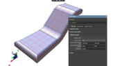
Designing microvias with sintered paste in rigid-flex PCBs offers enhanced electrical conductivity and mechanical strength, crucial for high-density applications. Our new article explores the benefits of sintered paste and provides essential design tips to optimize microvia performance and reliability.

Read More
Blog • Aug 14, 2024
Simple Strategies to Reach 10% PCB Cost Reduction

Our new article outlines strategies to achieve a 10% reduction in PCB costs by optimizing design and material choices, such as adjusting stack-up materials and hole sizes, using lower-cost parts, and considering single-sided assembly. These techniques help reduce expenses without sacrificing quality.

Read More
Blog • Aug 9, 2024
Say Goodbye to EDA Software Vendor Lock

Check how Altium 365 helps eliminate EDA software vendor lock by enabling multi-CAD support in the cloud. This allows users to work with different CAD file formats within a single platform, enhancing collaboration and reducing the need for additional licenses. This approach offers greater flexibility and is set to transform the industry.

Read More
Blog • Aug 7, 2024
The Ultimate Introduction to High-Speed Signal Integrity for PCB Designers

High-speed signal integrity is essential in PCB design to ensure data accuracy and system reliability. Key issues like impedance mismatches, crosstalk, and signal reflections need to be addressed through strategies such as controlled impedance traces, differential pairs, and suitable material choices. Check out our first article of the series about this topic.

Read More
Blog • Aug 5, 2024
Multi-Board PCB Signal Integrity: A Complete Guide

Our new article on signal integrity in multi-board PCBs covers essential aspects like connector pinouts, cable designs, and interconnect strategies. These factors ensure reliable performance in high-speed applications across industries such as military, aerospace, and AI.

Read More
Blog • Jul 30, 2024
Multi-CAD Support Will Be a Game Changer for Electronics Design Teams

Discover how multi-CAD support is transforming electronics design with Altium 365 by enabling seamless integration of diverse CAD file formats. This innovation addresses vendor lock-in issues, boosting collaboration, version control, and project management across different CAD tools.

Read More
  • Show More
Tag (field_common_tag)
Embedded thumbnail for Creating a PCB Footprint Courtyard
How to create a PCB Footprint • Jul 27, 2022
Creating a PCB Footprint Courtyard

The courtyard is an essential piece when you want to create a PCB Footprint in Altium Designer. We’ll talk about what a courtyard is, how to create a courtyard, and how to format a courtyard correctly for your PCB footprint.

Start Watching
Embedded thumbnail for How to Edit Existing Tracks in Altium Designer
How-To's • Jul 25, 2022
How to Edit Existing Tracks in Altium Designer

This new design rule flags a violation when the creepage distance across non-conductive surface and edge regions of the board, between the targeted signals, is equal to or less than the specified Creepage distance.

Start Watching
Embedded thumbnail for Creating a PCB Footprint Silkscreen Overlay
How to create a PCB Footprint • Jul 22, 2022
Creating a PCB Footprint Silkscreen Overlay

When creating a PCB footprint in Altium Designer creating a silkscreen overlay is an important requirement. We’ll go over the standards for creating a silkscreen overlay for a footprint and the steps to creating one, such as constructing lines and measuring distance of objects and primitives.

Start Watching
Embedded thumbnail for Adding Designators for Assembly Drawings
How-To's • Jul 18, 2022
Adding Designators for Assembly Drawings

Designators for assembly drawings are added on the assembly layer. This video shows how to add the designators.

Start Watching
Embedded thumbnail for Stackup Material Library
How to work with Layer Stack Manager • Jul 15, 2022
Stackup Material Library

In this video we will learn more about the Altium designers Layer Stack Mangers built-in materials library, and how to add new material and use it in our board stack. We will also look at how we can save the user materials to an xml format.

Start Watching
Embedded thumbnail for Placing Footprint Pads
How to create a PCB Footprint • Jul 13, 2022
Placing Footprint Pads

Every footprints needs proper pad placement to ensure trace connectivity. Placing pads is the first step towards footprint creation.

Start Watching
Embedded thumbnail for Setting the Transparency for Layers and Primitives
How-To's • Jul 11, 2022
Setting the Transparency for Layers and Primitives

Customize your workspace by setting the transparency of layers and primitives in the PCB.

Start Watching
Embedded thumbnail for Create New Via Types Using the Layer Stack Manager
How to work with Layer Stack Manager • Jul 8, 2022
Create New Via Types Using the Layer Stack Manager

In this video, we will learn how to create new via types using the Layer Stack Manager, and how to create new Routing Via design rules using the PCB Rules and Constraints Editor. We will also explore how to use the different types of Via during interactive routing.

Start Watching
Embedded thumbnail for How to Create a Copper Board Report
How-To's • Jul 4, 2022
How to Create a Copper Board Report

This video will show how to create a copper board report in your PCB which can be useful for copper balance in DFM process

Start Watching
Embedded thumbnail for Stackup Creation and editing
How to work with Layer Stack Manager • Jul 1, 2022
Stackup Creation and editing

This video shows how to view and edit the PCB Layer Stack, select materials and add new layers

Start Watching
Embedded thumbnail for Configuring Your PCB Library
How to create a PCB Footprint • Jun 29, 2022
Configuring Your PCB Library

It is important to have accurate footprints to manufacture your PCB. Learn how to configure your PCB library to facilitate footprint creation.

Start Watching
Embedded thumbnail for How to Validate Links Between Components and Footprints
How-To's • Jun 27, 2022
How to Validate Links Between Components and Footprints

Before importing or updating data from the circuit to the board, you must first verify that all components of the circuit are associated with Footprint. Watch this video to learn how to validate the links between your schematic components and footprints.

Start Watching
Embedded thumbnail for How to use Copy Room Format
How to work with Rooms • Jun 24, 2022
How to use Copy Room Format

Rooms allow you to use rules on specific areas of your design. This helps immensely with properly defining trace widths and hole sizes for specific components. We’ll show you how easy it is to assign rules to specific rooms in the PCB.

Start Watching
Embedded thumbnail for How To Do Versioning And Releases by Robert Feranec and Michal Faruga
Discovering Altium 365 • Jun 20, 2022
How To Do Versioning And Releases by Robert Feranec and Michal Faruga

Meet Robert Feranec in an educational video on version control, project history, comments, comparison and other features in Altium Designer 

Start Watching
Embedded thumbnail for Using Rooms in Rules
How to work with Rooms • Jun 17, 2022
Using Rooms in Rules

Rooms allow you to use rules on specific areas of your design. This helps immensely with properly defining trace widths and hole sizes for specific components. We’ll show you how easy it is to assign rules to specific rooms in the PCB.

Start Watching
Embedded thumbnail for Creating a Schematic Symbol: Dealing with Power Pins
How to create a Schematic Symbol • Jun 15, 2022
Creating a Schematic Symbol: Dealing with Power Pins

Multiple schematic symbols often require the use of multiple power and ground pins. We’ll show you the difference between hidden and visible power pins, and the various methods you can use to use them in your design however it works best for you.

Start Watching
  • Show More
Tag (field_common_tag)
 Preventing Obsolescence Before It Hits
On-Demand Webinar • Jun 12, 2025
Proactive Lifecycle Management: Preventing Obsolescence Before It Hits
Take the first step toward eliminating avoidable delays and costly redesigns. Don't miss it and register now!
Watch Now
Integrating Requirements June 2025 Webinar
On-Demand Webinar • May 28, 2025
Integrating Requirements into Your PCB Design Workflow
Join our webinar where you will learn about integrated requirements tools who can help you eliminate late-stage design changes, AI support through system requirements and integration of design requirements directly in PCB Design. Don't miss it, register now!
Watch Now
A365 Webinar
On-Demand Webinar • Apr 23, 2025
Collaborative Design Review: Ensuring Quality from Schematics to Supply Chain
Join our live webinar to learn how Altium 365 accelerates collaboration, standardizes workflows, and ensures design integrity to mitigate risks and accelerate time to market.
Watch Now
Webinar: From Prototype to Production: Optimizing BOM Costs Without Compromising Quality with Part Analytics
On-Demand Webinar • Apr 22, 2025
From Prototype to Production: Optimizing BOM Costs Without Compromising Quality with Part Analytics
Learn how to reduce production BOM costs without redesign, explore techniques to consolidate part demand for volume savings, and discover case examples from supply chain teams that increased sourcing process efficiency by up to 97%.
Watch Now
Streamlining Team Collaboration
On-Demand Webinar • Apr 17, 2025
Streamlining Team Collaboration in Industrial PCB Projects
Join us for our upcoming webinar to discover how Altium Designer and Altium 365 can transform your team’s collaboration and take your PCB design projects to the next level. Attend for a chance to win free access to the Altium 365 Training Bundle.
Watch Now
Component management
On-Demand Webinar • Apr 10, 2025
Ensure Best Designs with Professional Library Management
In this webinar, you'll discover how Altium Designer facilitates robust component management, including adding part choices to mitigate supply chain risks and leveraging Altium 365 managed components.
Watch Now
April 2025 Webinar Cover
On-Demand Webinar • Apr 9, 2025
Component Selection in Altium Designer: Making Data-Driven Decisions with Data Integrations
Improve component selection with real-time data insights in Altium 365! Join our live webinar to optimize your PCB development. Sign up now!
Watch Now
Altium Agile
Live Webinar
Altium Agile Teams - Sneak Peek
Get a first glimpse into this new Electronic Product Development Platform.
Jan
21
English
3:00 PM, CET
Jan
21
German
10:00 AM, CET
Jan
22
Italian
10:00 AM, CET
Jan
22
French
3:00 PM, CET
Jan
22
Spanish
3:00 PM, CET
Register Now
Altium Designer Overview
On-Demand Webinar • Dec 4, 2025
Altium Designer Onboarding Workshop
Join our live training workshop and see Altium Designer in action—from creating your first schematic to delivering ready-to-manufacture PCB files.
Watch Now
Altium Platform
On-Demand Webinar • Nov 21, 2025
Altium Platform - A foundation to meet your & your company’s targets
Discover how the Altium platform makes multidisciplinary cooperation easy and efficient.
Watch Now
Harness design
On-Demand Webinar • Nov 17, 2025
From single PCB to Harnessed Product
Discover how to streamline PCB-to-harness design with Altium’s powerful tools and boost collaboration across disciplines.
Watch Now
3D-MID Design
On-Demand Webinar • Oct 20, 2025
3D-MID Design in Altium
Discover how even complex products for 3D circuit designs are implemented easily in Altium.
Watch Now
Altium Designer Overview
On-Demand Webinar • Aug 20, 2025
Altium Designer and Altium 365 Overview
In this webinar we will show you how easy it is to create a prototype from scratch using Altium Designer in combination with Altium 365.
Watch Now
Altium Enterprise
On-Demand Webinar • Aug 3, 2025
Safety & Reliability in Electronics Design – Strategies, Standards & Tools
How can development teams and decision-makers effectively implement safety, security, and compliance without delaying innovation?
Watch Now
Altium Enterprise
On-Demand Webinar • Aug 2, 2025
Sustainability & Energy Efficiency in Electronic Product Development
Watch Now
Proactive Component Selection
On-Demand Webinar • May 22, 2025
Proactive Component Selection: Mitigating Manufacturing Delays Before They Happen
Most teams spend hours on component research yet still face redesigns. Learn how Altium 365 helps you make proactive, data-driven part decisions. Join SiliconExpert’s Jackie Sartin to discover smarter sourcing with real-time insights and validated alternatives.
Watch Now
  • Show More
Tag (field_common_tag)
Loading
Loading...
Share link
Share with
Search by Update
Version
Update
25 26 24 23 22
25.0 25.1 25.2 25.3 25.4 25.5 25.6 25.7 25.8 25.9
26.1 26.2
24.10 24.9 24.8 24.7 24.6 24.5 24.4 24.3 24.2 24.1 24.0
23.11 23.10 23.9 23.8 23.7 23.6 23.5 23.4 23.3 23.2 23.1 23.0
22.11 22.10 22.9 22.8 22.7 22.6 22.5 22.4 22.3