
Main navigation

  • Home
  • Discover
  • Learning Center
  • What’s New

Second main navigation

  • Altium Community
  • Support
  • Documentation
×

Results

  • Updates
  • Blog 570
  • Video 539
  • Webinar 86
  • Playlist 53
Filters:
Tag (field_common_tag)
Embedded thumbnail for Enhanced Constraint Manager in Altium Designer 25. Part I: From Directives to Creepage Rules
Enhanced Constraint Manager in Altium Designer 25 • Jun 9, 2025
Enhanced Constraint Manager in Altium Designer 25. Part I: From Directives to Creepage Rules

We are introducing a new video series on the Enhanced Constraint Manager in Altium Designer 25. In the first chapter, Samer Aldhaher demonstrates how to define net classes, apply clearance and creepage rules, and validate constraints within both the schematic and PCB. The video uses a 1kW, 400V brushless DC motor driver project to illustrate real-world applications.

Start Watching
Embedded thumbnail for Design Faster with Altium Designer 25
Altium Designer's 25 Quantitative Benefits • Jun 6, 2025
Design Faster with Altium Designer 25

Every second and every click count in the product development cycle. See how the new PCB Layout Replication feature in Altium Designer 25 boosts your efficiency in the PCB design process. Want to improve even more? Check out our Benefit Calculator now!

Start Watching
Embedded thumbnail for Creating PCB Drill Drawings and Tables in Altium Designer
How-To's • Jun 5, 2025
Creating PCB Drill Drawings and Tables in Altium Designer

If you want to learn more about drill drawings and tables in your PCB designs using Altium Designer, this tutorial is a must-watch. In the video, our Tech Consultant Zach Peterson walks you through multiple methods for generating these critical fabrication documents, including automatic Gerber outputs and custom drawings.

Start Watching
Embedded thumbnail for Streamlining Team Collaboration in Industrial PCB Projects - Recording Preview
New in Altium Designer 25 • Jun 4, 2025
Streamlining Team Collaboration in Industrial PCB Projects - Recording Preview

This webinar recording shows how Altium Designer and Altium 365 improve team collaboration in industrial PCB projects. It covers features like version control, live commenting, task tracking, and JIRA integration to help teams work more efficiently and reduce costly errors.

Start Watching
Blog • Jun 3, 2025
Preparing for Prototype: Final Component Validation

Final component validation is the last critical check before building a prototype, ensuring all parts are accurate, available, and viable. This article shows how Altium’s integrated tools—like SiliconExpert, Z2Data, Octopart, and BOM Portal—help teams avoid costly surprises and prepare with confidence.

Read More
Blog • Jun 2, 2025
Getting Started with Harness Design in Altium Designer 25

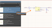
Explore the essential steps and tools for Harness Design in Altium Designer 25, from initial setup to final documentation. The article highlights how the unified design environment streamlines the entire process, improving efficiency and project integration.

Read More
Blog • May 30, 2025
The Future of PCB Design Starts Here

Altium Designer is constantly evolving, with powerful new features and updates on the way. Get an exclusive first look at what’s coming next—visit our Coming Soon page to stay up to date with the latest innovations.

Read More
Blog • May 29, 2025
Simplify Harness-to-System Connections for Better PCB Design Outcomes

Struggling to keep harness and system designs in sync? In our brand-new article we explore how integrating PCB and harness design workflows can eliminate errors, improve collaboration, and accelerate your development process. Discover a smarter approach to connecting your harness to the system.

Read More
Embedded thumbnail for AC Coupling Capacitors: Placement for High-Speed PCB Design
How-To's • May 28, 2025
AC Coupling Capacitors: Placement for High-Speed PCB Design

Learn the facts about AC coupling capacitor placement in high-speed PCB designs. In this video, Zach Peterson explores the ongoing debate: should AC coupling capacitors be placed near the transmitter or the receiver in high-speed differential pairs?

Start Watching
Blog • May 27, 2025
The Crucial Balance: Cost, Quality, and Availability In Electronic Component Selection

Balancing cost, quality, and availability is key when selecting electronic components. This article explores how to make informed choices that meet design goals while managing supply chain and sourcing challenges.

Read More
Embedded thumbnail for Coming Soon: Export 3D-MID Tracks as Centerline Curves
New in Altium Designer 25 • May 23, 2025
Coming Soon: Export 3D-MID Tracks as Centerline Curves

Coming Soon: 3D-MID Track-to-Centerline Export allows you to export conductive tracks on 3D substrates as precise centerline curves within STEP files—enabling seamless integration with advanced 5-axis manufacturing processes. Explore more upcoming upgrades on our Coming Soon page.

Start Watching
Embedded thumbnail for Advanced xSignal and Impedance Control Techniques - Recording Preview
New in Altium Designer 25 • May 20, 2025
Advanced xSignal and Impedance Control Techniques - Recording Preview

This webinar recording explores advanced xSignal and impedance control techniques in Altium Designer 25. It covers defining xSignals, managing impedance profiles, differential pairs, and delay tuning—all essential for high-speed PCB design. Full recording you find here: April 2025 COM Webinar Recording.

Start Watching
Blog • May 19, 2025
Wire Harness Failures: The Hidden Costs and Real-World Recalls That Could Have Been Prevented

Wire harness failures can lead to significant financial losses, production delays, and safety hazards. This article delves into real-world examples of such failures across industries and illustrates how modern CAD tools can help prevent these costly issues.

Read More
Embedded thumbnail for Coming Soon: Embedded 3D Models for Harness Designs
How-To's • May 16, 2025
Coming Soon: Embedded 3D Models for Harness Designs

Coming soon: the Embedded 3D Models for Harness Designs feature will automatically include Parasolid-format 3D models in your harness layout drawings. This improves integration with MCAD CoDesigner, enabling seamless synchronization between electrical and mechanical design domains. To see more upcoming upgrades, visit our Coming Soon page.

Start Watching
Embedded thumbnail for Make Smarter Design Decisions with Signal Analyzer by Keysight
New in Altium Designer 25 • May 14, 2025
Make Smarter Design Decisions with Signal Analyzer by Keysight

Discover how to simplify your workflow and boost design confidence with Signal Analyzer by Keysight—a complete extension available right inside Altium Designer 25. This whitepaper shows you how to analyze impedance, delay, and insertion/return loss without ever leaving your design environment.

Start Watching
Blog • May 13, 2025
Part Selection Fundamentals: Creating Resilient Component Requirements

Learn how to ensure electronic components meet the demands of harsh environments. This article explores key standards, testing protocols, and design considerations for building resilient systems that perform reliably under extreme conditions.

Read More
  • Show More
Tag (field_common_tag)
Why Use a Version Control System in PCB Design
Blog • Dec 17, 2021
Why Use a Version Control System in PCB Design

Version Control Systems (VCS) have been around for many decades within the software world but can be surprisingly new to some folks in the electronics design industry. This article will cover what a VCS is, what it does, and why you should be using one for your PCB design projects.

Read More
IPC 6012 Class 3 Annular Ring
Blog • Dec 16, 2021
Meeting Standards: IPC 6012 Class 3 Annular Ring

Designers often conflate leftover annular ring and pad sizes - they need to place a sufficiently large pad size on the surface layer to ensure that the annular ring that is leftover during fabrication will be large enough. As long as the annular ring is sufficiently large, the drill hit will not be considered defective and the board will have passed inspection. In this article, I'll discuss the limits on IPC-6012 Class 3 annular rings as these are a standard fabrication requirement for high-reliability rigid PCBs.

Read More
PCB fabrication notes
Blog • Dec 14, 2021
Decoding PCB Fabrication Notes

Sending a board out for fabrication is an exciting and nerve-wracking moment. Why not just give your fabricator your design files and let them figure it out? There are a few reasons for this, but it means the responsibility comes back to you as the designer to produce manufacturing files and documentation for your PCB. It’s actually quite simple if you have the right design tools. We’ll look at how you can do this inside your PCB layout and how this will help you quickly generate data for your manufacturer.

Read More
HDI PCB design and HDI PCB manufacturing process
Blog • Dec 9, 2021
Design Basics for HDI and the HDI PCB Manufacturing Process

As the world of technology has evolved, so has the need to pack more capabilities into smaller packages. PCBs designed using high-density interconnect techniques tend to be smaller as more components are packed in a smaller space. An HDI PCB uses blind, buried, and micro vias, vias in pads, and very thin traces to pack more components into a smaller area. We’ll show you the design basics for HDI and how Altium Designer® can help you create a powerful HDI PCB.

Read More
All About PCB Test Points
Blog • Dec 7, 2021
Is It Printed or a Component? All About PCB Test Points

Test points in your electronic assembly will give you a location to access components and take important measurements to verify functionality. If you’ve never used a test point or you’re not sure if you need test points, keep reading to see what options you have for test point usage in your PCB layout.

Read More
How to Design to a Differential Impedance Specification
Blog • Dec 2, 2021
How to Design to a Differential Impedance Specification

The concept and implementation of differential impedance are both sometimes misunderstood. In addition, the design of a channel to reach a specific differential impedance is often done in a haphazard way. The very concept of differential impedance is something of a mathematical construct that doesn’t fully capture the behavior of each signal in a differential trace. Keep reading to see a bit more depth on how to design to a differential impedance spec and exactly what it means for your design.

Read More
Draftsman Drawing
Blog • Nov 30, 2021
The Main Advantages when using Draftsman to Create a Component Mounting Drawing

Quite often, a standard assembly drawing is not enough to ensure the quality of a PCB assembly, especially when designing high-density boards. It would also be helpful to include additional detailing for simpler devices. The use of a Draftsman document brings an elegant, yet powerful solution to make these tasks easier.

Read More
Product Lifecycle Management in Electronics Manufacturing
Blog • Nov 25, 2021
Product Lifecycle Management in Electronics Manufacturing

An effective product lifecycle management (PLM) solution will integrate the tools and processes employed to design, develop and manufacture a new device. This solution goes beyond engineering activities to include the project management, process control, and financial management of the end-to-end business processes. PLM solutions create this collaborative environment where product development can flourish, bringing additional benefits in efficiencies and transparent communications, breaking silos, and speeding up the development process.

Read More
Tight versus loose coupling
Blog • Nov 23, 2021
Should You Use Tight vs. Loose Differential Pair Spacing and Coupling?

In this article, we want to get closer to a realistic description of tight coupling vs. loose coupling in terms of differential pair spacing, as well as how the differential pair spacing affects things like impedance, differential-mode noise, reception of common-mode noise, and termination. As we’ll see, the focus on tight coupling has its merits, but it’s often cited as necessary for the wrong reasons.

Read More
Engineering Design Review Guide
Blog • Nov 18, 2021
How to Solve Your Engineering Design Review Challenges

You’ve possibly gone through plenty of engineering design reviews, both on the front-end of a project and the back-end before manufacturing. Engineering design reviews are performed to accomplish multiple objectives, and with many engineering teams taking a systems-based approach to design and production, electronics design teams will need to review much more than just a PCB layout and BOM. Today’s challenges with sourcing, manufacturability, reliability, and mechanical constraints are all areas that must be confronted in real designs

Read More
Schematic Review Checklist
Blog • Nov 16, 2021
Schematic Review Checklist

One of the most common points of failure of a device occurs even before you start to layout your circuit board. Mistakes in your schematic design can easily make their way all the way into prototypes or production without a second thought once layout starts. In this article, I’m not going to extol the virtues of a good schematic design. Instead, this article is a simple no frills checklist.

Read More
Via current carrying capacity for PCBs
Blog • Nov 11, 2021
PCB Via Current-Carrying Capacity: How Hot is Too Hot?

One common question from designers is current-carrying capacity of conductors in a PCB. Trace and via current-carrying capacity are legitimate design points to focus on when designing a new board that will carry high current. The goal is to keep conductor temperatures below some appropriate limit, which then helps keep components on the board cool. Let’s dig into the current state of thermal demands on vias in PCBs and how they compare to internal and external PCB traces.

Read More
PCB Shield
Blog • Nov 9, 2021
Phalanx, not Failure: PCB Shielding to Protect Your Design

A combination of good printed circuit board design and good shielding mitigates EMI. Good PCB design for EMI shielding revolves around the layout, the placement of filters, and ground planes. A well-designed PCB minimizes parasitic capacitance and ground loops. Keep reading to learn more about PCB shielding.

Read More
Man working in Altium Designer
Blog • Nov 4, 2021
Best Practices in Hardware Version Control Systems

Any project can get very complex, and the PCB design team needs to track revisions throughout a project. Why worry about tracking revisions? In the event you ever receive changes to product functional requirements, major changes are made to your product’s architecture, or you’re ready to finalize the design and prepare for fabrication, it’s best to clone a project at its current state and begin working on a new version. Keeping track of all these design changes in a PCB design project takes the type of hardware version control tools you’ll find in Altium 365™.

Read More
Copper pour and via stitching
Blog • Oct 28, 2021
Copper Pour and Via Stitching: Do You Need Them in a PCB Layout?

To pour or not to pour, to stitch or not to stitch… Over many years, some common “rules of thumb” have become very popular and, ultimately, taken a bit out of context. Rules of thumb are not always wrong, but taking PCB design recommendations out of context helps justify bad design practices, and it can even affect the producibility of your board. Like many aspects of a physical PCB layout, via stitching and copper pour can be like acid: quite useful if implemented properly, but also dangerous if used indiscriminately.

Read More
MOSFET Components
Blog • Oct 26, 2021
Should You Use Power MOSFETs in Series?

Power MOSFETs enable a huge range of electronic systems, specifically in situations where BJTs are not useful or efficient. MOSFETs can be used in high current systems in parallel arrangements, but what about their use in series? Both arrangements of MOSFETs have their pitfalls that designers should consider. Let’s look at MOSFETs in series as they are quite useful in certain systems, but be careful to design your circuits and your PCB for reliability.

Read More
  • Show More
Tag (field_common_tag)
Embedded thumbnail for PCB Stackups in Reverse?
How-To's • Apr 21, 2025
PCB Stackups in Reverse?

Watch our new tutorial on reverse PCB stackups — a unique approach that combines thin internal layers with thicker outer cores for specialized applications. Learn how to implement reverse stackups effectively in Altium Designer, understand key manufacturability constraints, and explore Rogers materials specifically suited for this technique.

Start Watching
Embedded thumbnail for Design Smarter - Harness, Multi-board, and MCAD CoDesign in Action
New in Altium Designer 25 • Apr 16, 2025
Design Smarter - Harness, Multi-board, and MCAD CoDesign in Action

This webinar highlights how Altium Designer 25, with a Pro or Enterprise subscription, enables seamless ECAD-MCAD collaboration using Harness and Multi-board Design tools and the advanced MCAD CoDesigner. Viewers will learn how to integrate harness designs, optimize multi-board systems for enclosure fit, and synchronize designs with SolidWorks, PTC Creo, and Autodesk Inventor.

Start Watching
Embedded thumbnail for Unified Login in Altium Designer 25
New in Altium Designer 25 • Apr 14, 2025
Unified Login in Altium Designer 25

We've unified the login experience across Altium Designer, Altium 365, and the Altium website—one set of credentials is all you need. This update simplifies access, enhances security, and improves session management for a smoother user experience.

Start Watching
Embedded thumbnail for Custom Ethernet Switch Powers Up: Assembly to Working Hardware Test
How-To's • Apr 11, 2025
Custom Ethernet Switch Powers Up: Assembly to Working Hardware Test

Watch our latest video as host Zach Peterson presents his custom Ethernet switch PCB. He walks through the design in Altium Designer, programs the firmware, and tests the board in a real server environment using both copper and fiber connections. This video showcases the complete journey from PCB design to fully functional hardware.

Start Watching
Embedded thumbnail for Mastering Pad and Via Templates (or Padstacks) in Altium Designer
How-To's • Apr 1, 2025
Mastering Pad and Via Templates (or Padstacks) in Altium Designer

Learn how to create, export, and reuse Pad and Via templates (Padstacks) in Altium Designer. This tutorial covers standardized libraries to optimize PCB design and ensure consistency across projects.

Start Watching
Embedded thumbnail for Power Rail Routing Mastery: Multiple Voltage Planes in Altium Designer
How-To's • Mar 28, 2025
Power Rail Routing Mastery: Multiple Voltage Planes in Altium Designer

Want to design a complex Power Distribution Network (PDN)? Watch our exclusive tutorial to learn expert techniques for routing 10+ power rails on a single PCB layer—while minimizing EMI and ensuring signal integrity.

Start Watching
Embedded thumbnail for Unveiling 99% Task Time Efficiency
Altium Designer's 25 Quantitative Benefits • Mar 27, 2025
Unveiling 99% Task Time Efficiency

This video showcases Altium Designer 25’s PCB Section View, a powerful tool for detailed circuit analysis and optimization. Learn how it enhances precision, improves performance, and simplifies complex PCB layouts with real-world applications.

Start Watching
Embedded thumbnail for Bottom Terminated Component Guide: Footprint Design Best Practices
How-To's • Mar 21, 2025
Bottom Terminated Component Guide: Footprint Design Best Practices

Want to create a reliable footprint for your PCB design? Watch our latest video with Zach Peterson and learn best practices for designing PCB footprints for bottom-terminated components. This tutorial covers how to properly design paste masks for QFNs, BGAs, and other bottom-terminated packages to prevent common assembly issues.

Start Watching
Embedded thumbnail for Design 4x Faster with Altium Designer 25
Altium Designer's 25 Quantitative Benefits • Mar 20, 2025
Design 4x Faster with Altium Designer 25

PCB CoDesign in Altium Designer 25 enables multiple engineers to collaborate on a single PCB design, saving over 10 minutes and 300+ clicks. With an intuitive compare-and-merge workflow, teams can efficiently resolve conflicts and streamline their design process. Check out this video to learn more, and use the Benefit Calculator to see your potential time savings: https://www.altium.com/benefit-calculator.

Start Watching
Embedded thumbnail for Empowering Hybrid Designs with Wire Bonding
New in Altium Designer 25 • Mar 18, 2025
Empowering Hybrid Designs with Wire Bonding

Our latest whitepaper on Wire Bonding technology is now available! It explores the role of wire bonding in modern PCB design and how Altium Designer 25 enhances the process with dedicated features. Access it here: Wire Bonding Whitepaper.

Start Watching
Embedded thumbnail for 8 Times Faster Simulations Using Altium Designer 25
Altium Designer's 25 Quantitative Benefits • Mar 14, 2025
8 Times Faster Simulations Using Altium Designer 25

Speed up your simulations with Altium Designer 25—now up to 8x faster! Watch our comparison to see how built-in simulation slashes processing time, saving you valuable minutes on every task.

Start Watching
Embedded thumbnail for Harness Design Top 5 Improvements in Altium Designer 25
New in Altium Designer 25 • Mar 12, 2025
Harness Design Top 5 Improvements in Altium Designer 25

Harness Design in Altium Designer 25 just got a major upgrade! This video showcases the top five new features that improve flexibility, organization, and efficiency in your wiring workflow. Watch now to see these enhancements in action and take your designs to the next level!

Start Watching
Embedded thumbnail for HitIQ uses Altium solutions to better understand brain injuries in sports sciences
Altium Stories • Mar 7, 2025
HitIQ uses Altium solutions to better understand brain injuries in sports sciences

Watch our video about HitIQ and theirs usage of Altium's software to develop a Smart Mouthguard, an advanced concussion management solution. Our software accelerated their development, improved accuracy, and its helpful for detecting and managing sports-related brain injuries.

Start Watching
Embedded thumbnail for Boost Team Productivity with Seamless Collaboration - Recording Preview
New in Altium Designer 25 • Mar 5, 2025
Boost Team Productivity with Seamless Collaboration - Recording Preview

Discover how to enhance your PCB design workflow with Altium Designer and Altium 365. Learn to speed up tasks, enhance collaboration, connect teams, and optimize part selection—all in one seamless environment.

Start Watching
Embedded thumbnail for Altium Tutorial: Harness Design to Multi-Board Assembly Workflow
How-To's • Feb 28, 2025
Altium Tutorial: Harness Design to Multi-Board Assembly Workflow

Watch our latest tutorial on Harness Design and Multi-board, where we showcase best practices for Harness Design, MCAD collaboration, and manufacturing documentation generation to enhance your PCB assembly workflow.

Start Watching
Embedded thumbnail for Smart Mouthguard Impacting Concussion Science
Altium Stories • Feb 26, 2025
Smart Mouthguard Impacting Concussion Science

Check out our latest Customer Success Story about HitIQ, founded by former AFL player Nathan Murphy. HitIQ harnessed Altium’s design and collaboration tools to develop its Smart Mouthguard—an advanced concussion management solution. The team utilized Altium Designer’s Rigid-Flex PCB capabilities and Constraint Manager, along with Altium 365’s Web Viewer and Cloud Storage, to create a compact yet highly functional design while enhancing cross-functional collaboration.

Start Watching
  • Show More
Tag (field_common_tag)
ADv25
On-Demand Webinar • Oct 24, 2024
Modernizing Engineering Workflows: Altium Designer 25 and the Future of Concurrent Design
Struggling with team misalignment and design errors? Join our exciting webinar to discover the groundbreaking advancements in Altium Designer 25!
Watch Now
KiCad Webinar
On-Demand Webinar • Oct 16, 2024
Taking the Next Step: Growing Beyond KiCad with Altium
Join our upcoming webinar to discover how Altium Designer can transition your KiCad projects without any data loss
Watch Now
Synchronize to Optimize Jira Integration
On-Demand Webinar • Oct 7, 2024
Synchronize to Optimize: Enhancing Efficiency with Jira Integration for Altium 365
Tired of juggling multiple tools for project management? Watch the webinar and see how Jira Integration for Altium 365 can optimize your workflows.
Watch Now
Wire bonding
On-Demand Webinar • Sep 29, 2024
Unlock New Design Possibilities with Wire Bonding
Explore how wire bonding can enhance your designs, provide size reduction, improve power management, and increase mechanical reliability.
Watch Now
routing
On-Demand Webinar • Sep 29, 2024
Advanced Routing Features & Techniques
To help you get the most out of your experience with Altium Designer, join our webinar this month and learn advanced routing techniques.
Watch Now
signal analyzer
On-Demand Webinar • Sep 25, 2024
Signal Integrity Made Simple
Discover how to easily detect and resolve high-speed signal integrity challenges without the need for extensive expertise.
Watch Now
competitive-displacement-webinar-3
On-Demand Webinar • Sep 20, 2024
Mastering Design Complexity: How Altium Designer Outperforms Cadence in Solving Workflow and Engineering Challenges - Part 2
Join our webinar to learn how to enhance efficiency, foster better collaboration, and accelerate your time-to-market with Altium unified solutions.
Watch Now
Breaking Down Silos Webinar
On-Demand Webinar • Sep 16, 2024
Breaking Down Data Silos: A Practical Comparison of Altium and Cadence in Cross-Functional PCB Design
Join us for a webinar that addresses the critical challenges of maintaining design data continuity across various design functions.
Watch Now
Draftsman
On-Demand Webinar • Sep 10, 2024
Mastering Design Complexity: How Altium Designer Outperforms Cadence in Solving Workflow and Engineering Challenges
Join our upcoming webinar to discover why engineers consistently choose Altium Designer as the standard in PCB design.
Watch Now
SPICE
On-Demand Webinar • Sep 3, 2024
Mastering SPICE Simulation in Altium Designer
Discover how the SPICE engine in Altium Designer can help you easily verify that your finished project functions as intended.
Watch Now
Output job
On-Demand Webinar • Aug 24, 2024
Beyond PCB Design with Altium Designer
In this webinar we'll dive into the essential aspects that go beyond the schematic and layout.
Watch Now
PCB
On-Demand Webinar • Aug 23, 2024
Elevate Your Design Skills: Tips & Tricks for Success
Discover practical insights and efficient methods that can enhance your PCB design capabilities.
Watch Now
Cyber Security Webinar Cover
On-Demand Webinar • Aug 6, 2024
The Anatomy of IT Compliance in Electronics Development: Altium 365 & AWS GovCloud
Are you an IT or security professional looking for a secure electronics design collaboration platform that could also support your ITAR and EAR compliance efforts? If so, watch this webinar to bring together the expertise of Altium 365 and AWS!
Watch Now
Design reuse
On-Demand Webinar • Aug 1, 2024
How to Speed-up Product Development with Reusable Circuitry
In this webinar you'll learn more about the benefits of the design reuse blocks approach as well as the Design Reuse panel.
Watch Now
Harness design
On-Demand Webinar • Jul 19, 2024
Stay Ahead of the Curve: A Half-Year Review of Altium Designer Improvements
Join our exciting webinar to discover the groundbreaking advancements in Altium Designer!
Watch Now
Lenght Tuning
On-Demand Webinar • Jun 26, 2024
Achieve Precision and Speed with Altium Designer 24's Innovative Routing Features
Speed up your routing process and achieve better results for even your most demanding designs.
Watch Now
  • Show More
Tag (field_common_tag)
Loading
Loading...
Share link
Share with
Search by Update
Version
Update
25 26 24 23 22
25.0 25.1 25.2 25.3 25.4 25.5 25.6 25.7 25.8 25.9
26.1 26.2
24.10 24.9 24.8 24.7 24.6 24.5 24.4 24.3 24.2 24.1 24.0
23.11 23.10 23.9 23.8 23.7 23.6 23.5 23.4 23.3 23.2 23.1 23.0
22.11 22.10 22.9 22.8 22.7 22.6 22.5 22.4 22.3