
Main navigation

  • Home
  • Discover
  • Learning Center
  • What’s New

Second main navigation

  • Altium Community
  • Support
  • Documentation
×

Results

  • Updates
  • Blog 571
  • Video 540
  • Webinar 86
  • Playlist 53
Filters:
Tag (field_common_tag)
Embedded thumbnail for Auto-tuning Your Way to Faster PCB Design
Altium Designer's 25 Quantitative Benefits • Jun 13, 2025
Auto-tuning Your Way to Faster PCB Design

Watch how the Auto Tuning feature in Altium Designer 25 delivers optimized DDR4 routing in a single click! Fewer steps, massive time savings. Try our Benefit Calculator to estimate your own time and cost savings.

Start Watching
Blog • Jun 12, 2025
Twice the Insight. One Seamless Simulation Bundle

Ensure power and signal integrity with the Keysight Bundle in Altium Designer. Catch issues early, reduce rework, and optimize your PCBs - all within one integrated environment featuring Signal & Power Analyzer.

Read More
Embedded thumbnail for Enhanced Constraint Manager in Altium Designer 25. Part I: From Directives to Creepage Rules
Enhanced Constraint Manager in Altium Designer 25 • Jun 9, 2025
Enhanced Constraint Manager in Altium Designer 25. Part I: From Directives to Creepage Rules

We are introducing a new video series on the Enhanced Constraint Manager in Altium Designer 25. In the first chapter, Samer Aldhaher demonstrates how to define net classes, apply clearance and creepage rules, and validate constraints within both the schematic and PCB. The video uses a 1kW, 400V brushless DC motor driver project to illustrate real-world applications.

Start Watching
Embedded thumbnail for Design Faster with Altium Designer 25
Altium Designer's 25 Quantitative Benefits • Jun 6, 2025
Design Faster with Altium Designer 25

Every second and every click count in the product development cycle. See how the new PCB Layout Replication feature in Altium Designer 25 boosts your efficiency in the PCB design process. Want to improve even more? Check out our Benefit Calculator now!

Start Watching
Embedded thumbnail for Creating PCB Drill Drawings and Tables in Altium Designer
How-To's • Jun 5, 2025
Creating PCB Drill Drawings and Tables in Altium Designer

If you want to learn more about drill drawings and tables in your PCB designs using Altium Designer, this tutorial is a must-watch. In the video, our Tech Consultant Zach Peterson walks you through multiple methods for generating these critical fabrication documents, including automatic Gerber outputs and custom drawings.

Start Watching
Embedded thumbnail for Streamlining Team Collaboration in Industrial PCB Projects - Recording Preview
New in Altium Designer 25 • Jun 4, 2025
Streamlining Team Collaboration in Industrial PCB Projects - Recording Preview

This webinar recording shows how Altium Designer and Altium 365 improve team collaboration in industrial PCB projects. It covers features like version control, live commenting, task tracking, and JIRA integration to help teams work more efficiently and reduce costly errors.

Start Watching
Blog • Jun 3, 2025
Preparing for Prototype: Final Component Validation

Final component validation is the last critical check before building a prototype, ensuring all parts are accurate, available, and viable. This article shows how Altium’s integrated tools—like SiliconExpert, Z2Data, Octopart, and BOM Portal—help teams avoid costly surprises and prepare with confidence.

Read More
Blog • Jun 2, 2025
Getting Started with Harness Design in Altium Designer 25

Explore the essential steps and tools for Harness Design in Altium Designer 25, from initial setup to final documentation. The article highlights how the unified design environment streamlines the entire process, improving efficiency and project integration.

Read More
Blog • May 30, 2025
The Future of PCB Design Starts Here

Altium Designer is constantly evolving, with powerful new features and updates on the way. Get an exclusive first look at what’s coming next—visit our Coming Soon page to stay up to date with the latest innovations.

Read More
Blog • May 29, 2025
Simplify Harness-to-System Connections for Better PCB Design Outcomes

Struggling to keep harness and system designs in sync? In our brand-new article we explore how integrating PCB and harness design workflows can eliminate errors, improve collaboration, and accelerate your development process. Discover a smarter approach to connecting your harness to the system.

Read More
Embedded thumbnail for AC Coupling Capacitors: Placement for High-Speed PCB Design
How-To's • May 28, 2025
AC Coupling Capacitors: Placement for High-Speed PCB Design

Learn the facts about AC coupling capacitor placement in high-speed PCB designs. In this video, Zach Peterson explores the ongoing debate: should AC coupling capacitors be placed near the transmitter or the receiver in high-speed differential pairs?

Start Watching
Blog • May 27, 2025
The Crucial Balance: Cost, Quality, and Availability In Electronic Component Selection

Balancing cost, quality, and availability is key when selecting electronic components. This article explores how to make informed choices that meet design goals while managing supply chain and sourcing challenges.

Read More
Embedded thumbnail for Coming Soon: Export 3D-MID Tracks as Centerline Curves
New in Altium Designer 25 • May 23, 2025
Coming Soon: Export 3D-MID Tracks as Centerline Curves

Coming Soon: 3D-MID Track-to-Centerline Export allows you to export conductive tracks on 3D substrates as precise centerline curves within STEP files—enabling seamless integration with advanced 5-axis manufacturing processes. Explore more upcoming upgrades on our Coming Soon page.

Start Watching
Embedded thumbnail for Advanced xSignal and Impedance Control Techniques - Recording Preview
New in Altium Designer 25 • May 20, 2025
Advanced xSignal and Impedance Control Techniques - Recording Preview

This webinar recording explores advanced xSignal and impedance control techniques in Altium Designer 25. It covers defining xSignals, managing impedance profiles, differential pairs, and delay tuning—all essential for high-speed PCB design. Full recording you find here: April 2025 COM Webinar Recording.

Start Watching
Blog • May 19, 2025
Wire Harness Failures: The Hidden Costs and Real-World Recalls That Could Have Been Prevented

Wire harness failures can lead to significant financial losses, production delays, and safety hazards. This article delves into real-world examples of such failures across industries and illustrates how modern CAD tools can help prevent these costly issues.

Read More
Embedded thumbnail for Coming Soon: Embedded 3D Models for Harness Designs
How-To's • May 16, 2025
Coming Soon: Embedded 3D Models for Harness Designs

Coming soon: the Embedded 3D Models for Harness Designs feature will automatically include Parasolid-format 3D models in your harness layout drawings. This improves integration with MCAD CoDesigner, enabling seamless synchronization between electrical and mechanical design domains. To see more upcoming upgrades, visit our Coming Soon page.

Start Watching
  • Show More
Tag (field_common_tag)
How I Improved My Collaboration Efficiency with Altium 365
Blog • Nov 8, 2022
How I Improved My Collaboration Efficiency with Altium 365

Involving the whole team that will bring a product to completion early on in the development cycle is vital to efficient development. Design reviews with all the relevant parties are critical at each step of the design process, starting with high-level component selection, then through the schematic capture and PCB layout stages. 

Read More
Countersink and Counterbore
Blog • Nov 3, 2022
Countersink and Counterbore

Ergonomics and convenience are important issues when designing a printed circuit board and the device as a whole. A lot of Altium Designer tools are aimed at solving them. These include Countersink and Counterbore holes, which allow the use of various types of screws in the mounting holes of the board.

Read More
Migrating Data From Other Version Control Systems
Blog • Nov 1, 2022
Migrating Data From Other Version Control Systems

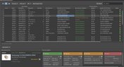
The development of electronic devices always involves the release of many different types of files. And these files are not static - they change as the project progresses. When filling a project with data, a user creates new files, modifies outdated files that have become irrelevant. Managing project data is a separate task, especially for large developments where several participants with different specializations are involved in the process.

Read More
Properties Panel Tuning
Blog • Oct 27, 2022
Properties Panel Tuning

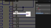
High-speed PCBs often require tuning groups of tracks, both single and differential. Altium Designer includes powerful tools that allow you to solve such tasks quickly and with high quality. Study this document and achieve the desired result even faster.

Read More
Reflectionless Matching vs. Conjugate Matching: An Apparent Contradiction
Blog • Oct 25, 2022
Reflectionless Matching vs. Conjugate Matching: An Apparent Contradiction

There is one confusion related to impedance matching that comes up again and again, and it appears to be a fundamental confusion between reflection and power delivery. This leads to an apparent contradiction that arises when we try to generalize power delivery to wave reflection, despite the fact that the two were not meant to be related.

Read More
Properties Panel Routing
Blog • Oct 20, 2022
Properties Panel Routing

Routing is one of the most time-consuming stages of PCB design. Altium Designer has a large set of tools that allow you to do it as accurately and quickly as possible. This document will help you to learn how to manage your routing effectively and use it to its fullest extent.

Read More
Quarter-Wave Transformer Design For Real and Reactive Loads
Blog • Oct 18, 2022
Quarter-Wave Transformer Design For Real and Reactive Loads

RF systems operate with specific impedance values across entire interconnects, including on PCBs. Not all RF components are packaged in integrated circuits with defined impedances, so impedance matching circuits and line sections are needed to ensure signal transmission between different sections of an interconnect. One of these impedance matching techniques is the quarter-wave impedance transformer, which can be implemented as a printed trace with specific impedance.

Read More
Schematic
Blog • Oct 14, 2022
Altium Designer 22.10 Update

We are happy to announce that the Altium Designer 22.10 update is now available. Altium Designer 22.10 continues to focus on improving the user experience, as well as performance and stability of the software, based on feedback from our users. Check out the key new features in the What's New section on the left side of this window!

Read More
Component Warpage Causes in a PCB
Blog • Oct 13, 2022
Component Warpage Causes in a PCB

A staff member at a PCB manufacturer once explained to me that they thought we were having an issue with a package warping. Unfortunately, component warping can occur both in a PCB and in components. In this article, we'll give an overview of warpage in a PCB, specifically in the circuit board and in the components.

Read More
Link Budget Calculator
Blog • Oct 11, 2022
RF Signal Chain and Link Budget Basics

If you're designing a wireless IoT device, and you know how to calculate the link budget, you can reasonably estimate whether your signal will reach its destination and be read by the receiver. To calculate the link budget, the designer needs to know something about all other sources of gain and loss in the system. Once link budget is determined, the designer can judge whether some modification is needed in their RF signal chain. 

Read More
How to Calculate SMD Pad Sizes?
Blog • Oct 6, 2022
Best Methods for Calculating SMD Pad Size in PCB Design

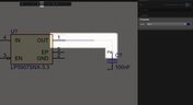
SMD components require precisely sized pads for soldering during assembly. The designer is responsible for ensuring pad sizes are correct, either by calculating them and comparing with footprint data, looking through datasheets, or by memorizing SMD pad size standards. If you have a component and you don't have access to the footprint, and you decide to biuld the footprint yourself, what resources are available to ensure you have the correct pad size?

Read More
Can You Fix a Warped PCB?
Blog • Oct 4, 2022
Can You Fix a Warped PCB?

Before we get too deep into this article, I’ll give you the simple answer. You probably can’t fix warping in your PCB after it’s already been fabricated. You can prevent an unwarped board from becoming warped during assembly, but only as long as materials were selected properly and the board is put into reflow correctly. We’ll run over some of these points in this article, and I’ll examine some points that might help you recover a warped board.

Read More
What is an Eye Diagram?
Blog • Sep 29, 2022
What is an Eye Diagram?

The eye diagram is a useful measurement or simulation as part of channel compliance. The measurement shows many different factors that can affect signal behavior simultaneously, ultimately allowing for qualification of errors and losses in a channel. In this article, I’ll run over some of the fundamental measurements that you could manually extract from an eye diagram and how they reveal some strategies for improving channel designs.

Read More
Skills for Today's PCB Designers
Blog • Sep 27, 2022
What Skills Are Needed to be a PCB Layout Designer?

To readers who have been working in the PCB industry for most of your career, you have probably seen a very diverse group of professionals with varied skill sets and backgrounds. Designers might get started as engineers or as technicians, and some designers learn how to create beautiful PCB layouts in university. No matter how you got into PCB design, there are some important skills to know that will take you a long way towards advancing your career.

Read More
How to Fix the Top PCB Design Mistakes
Blog • Sep 22, 2022
Beginner PCB Design Mistakes and How To Avoid Them

When starting out with PCB design, it’s common to treat the process as simply ‘connecting the dots’: as long as connections are made, it’s not particularly important how these connections are made. Having reviewed quite a number of PCBs of other PCB design engineers over the last few years, there are common, unfortunately erroneous, occurrences between a lot of them. This article aims to illustrate the top five beginner PCB design mistakes and what we can do to avoid making them. Let’s get started!

Read More
Top 5 Questions Regarding Stack Up
Blog • Sep 20, 2022
SAP (Semi-Additive PCB Process) – Top 5 Questions Regarding Stack Up

As the PCB design community embraces the benefits of this new printed circuit board fabrication technique, there are of course many questions to be answered.  Today’s blog will address some of the most commonly asked questions related to circuit layer stack up as people are introduced to this new technology.

Read More
  • Show More
Tag (field_common_tag)
Embedded thumbnail for New Routing Capabilities
New in Altium Designer 20 • Apr 23, 2020
New Routing Capabilities

Advanced routing capabilities help you complete the most basic, as well as the most difficult, routing challenges. In Altium Designer 20.0, we’ve added intelligent control over pad entries that are capable of working with any combination of pad geometry as well as a new any angle routing mode that allows you to make beautiful traces that smoothly contours around obstacles.

Start Watching
Embedded thumbnail for New Length Tuning Engine
New in Altium Designer 20 • Apr 21, 2020
New Length Tuning Engine

The tuning engine in Altium Designer has been redesigned and is now better than ever. Tuning sections can be picked up and moved to new locations on the track. What is truly remarkable is that the tunings are completely dynamic and change shape and fill patterns depending on the boundaries and surroundings.

Start Watching
Embedded thumbnail for Using the ActiveBOM
• Apr 20, 2020
Using the ActiveBOM

The Bill of Materials (BOM) contains a list of all the components with their designators, part numbers, values, and other parameters. An ActiveBOM manages the mapping from the design component (part) to the part that is purchased. This video descibes how to use the ActiveBOM document to create an up-to-date list of components needed for your project.

Start Watching
Embedded thumbnail for Wiring The Schematic
• Apr 20, 2020
Wiring The Schematic

This video demonstrates how to wire the schematic before it is transferred to the PCB. The Wire tool on the Active Bar or Place menu is activated and used to place wires. The video also shows how to add intermediate points along the wire route in order to more accurately route the wire.

Start Watching
Embedded thumbnail for Schematic Component Placement
• Apr 20, 2020
Schematic Component Placement

This video demonstrates how the Components panel is used to find and place components on the schematic. To search for components and filter the Components panel results, enter the component name in the Search field of the panel. The desired component appears in the filtered list and can now be placed by clicking and dragging, double-clicking on the desired component, or by right-clicking on the component then selecting Place from the context menu.

Start Watching
Embedded thumbnail for Resolving Schematic Errors
• Apr 20, 2020
Resolving Schematic Errors

So, you’ve validated your project and you’ve noticed that you have several errors and warnings, but you’re not sure where you went wrong. So we’ll be showing you some common violations, why they appeared, and how to correct them.

Start Watching
Embedded thumbnail for Searching for Errors
• Apr 20, 2020
Searching for Errors

Errors and mistakes happen to everyone - from beginners to professionals. So we always preach how its paramount for your design to be validated before pushing it to the PCB. But luckily it’s pretty easy to find and analyze any errors using Altium Designer. We’ll take a look at how to find and analyze errors in your schematic.

Start Watching
Embedded thumbnail for Schematic Port Placement
• Apr 20, 2020
Schematic Port Placement

A port is an electrical design primitive that is used to make an electrical connection between schematic sheets. The connection is made through the name of the ports on each sheet. This video shows how to place ports from the Place menu or the Active Bar, then configure the port Name, I/O Type, width, and output symbols.

Start Watching
Embedded thumbnail for Schematic Annotation
• Apr 20, 2020
Schematic Annotation

Annotation assigns designators to all or selected parts in selected sheets and ensures that designators are unique and ordered based on their position. This video demonstrates the quick and easy process for annotating schematics quietly in Altium Designer. The Annotate Schematics Quietly command used in the video applies all previous settings of the Annotate dialog without needing to reopen the dialog.

Start Watching
Embedded thumbnail for Using Net Labels
• Apr 20, 2020
Using Net Labels

Assigning names to nets has many uses, including assisting in documenting circuit design as well as providing a reference for design rules in the PCB. In this video, we demonstrate how to place net names (labels) using the Place menu. The Properties panel is then used to enter the net name.

Start Watching
Embedded thumbnail for Using Power Ports
• Apr 20, 2020
Using Power Ports

In this video, you will be shown how to place and configure power ports. Using the Power Port tool located on the Active Bar or on the Place menu, place the required power ports in the desired locations. The Properties panel can be used to set the name, style, etc., of the power port during or after placement.

Start Watching
Embedded thumbnail for Manufacturer Part Search
• Apr 20, 2020
Manufacturer Part Search

This video demonstrates how to find and place parts that are not available in your cloud or local libraries using the Manufacturer Part Search panel. The Manufacturer Part Search panel is powered by Octopart technologies and has a powerful search and filter feature based on categories and parametric filtering that allows you to zero in on the exact manufactured component you need. Once the correct part is found, you can place the part using a few clicks; you can also download or acquire the part for local use in your future designs.

Start Watching
Embedded thumbnail for Schematic Grids and Preferences
• Apr 20, 2020
Schematic Grids and Preferences

Before you start designing in the schematic environment, there are a few things you need to consider. One of those considerations would be setting your schematic grid. In this video, we'll cover how to configure different types of grids in Altium Designer.

Start Watching
Embedded thumbnail for Interaction with Projects
• Apr 20, 2020
Interaction with Projects

When you’re first starting to design your project, you should be asking yourself a few questions in regard to your project’s structure. So in this video, we’ll break down how we use a Project to represent a full design, and how we can add documents to it, such as a schematic sheet.

Start Watching
Embedded thumbnail for How to Assign Names to Polygons
Working with Polygons • Apr 3, 2020
How to Assign Names to Polygons

For some polygons, it is not always reasonable to use an automatically generated name so a custom name is needed. With a proper polygon name, you can quickly find the desired polygon in a list and correctly set the pour priority in relation to other polygons. By using unique names, you can create design rules that apply only to specified polygons.

Start Watching
Embedded thumbnail for How to Use View Mode in Altium Designer Without a License
How-To's • Mar 16, 2020
How to Use View Mode in Altium Designer Without a License

In Altium Designer 20.0, you can use Altium Designer in Viewer mode when signed into your AltiumLive account and no active license is being used. The Altium Designer Viewer license can be used by anyone with an AltiumLive account and no other licenses or subscription is needed. The license can be activated from the License Management page. 

Start Watching
  • Show More
Tag (field_common_tag)
Altium Enterprise
On-Demand Webinar • May 10, 2025
Streamline your customer relation with Altium 365 Enterprise
Join our webinar designed for engineers and users in EMS companies
Watch Now
PCB
On-Demand Webinar • May 1, 2025
Altium Designer Overview
Altium Designer is the #1 PCB design tool for a reason. Join us for this live webinar and get an inside look at Altium’s world-class PCB design solution. See for yourself why design teams around the globe are making the switch to Altium Designer. Register now!
Watch Now
Enterprise
On-Demand Webinar • Apr 25, 2025
Altium Customization with Scripting or Low-Code
See how scripting, low-code, no-code, and API integrations can help you work more efficiently—without extra setup or complex systems.
Watch Now
A365 Webinar: Altium BOM Portal - From PCB Design to Parts Ordering in Minutes
On-Demand Webinar • Apr 21, 2025
Altium 365 BOM Portal - From PCB Design to Parts Ordering in Minutes
Join us to learn how to reduce sourcing time by up to 70% using Altium 365 BOM Portal.
Watch Now
April 2025 COM Webinar
On-Demand Webinar • Apr 17, 2025
Advanced xSignal and Impedance Control Techniques
We are hosting a free webinar on advanced xSignal configuration and impedance control techniques in Altium Designer to help you tackle signal integrity challenges. Register now to enhance your design skills.
Watch Now
Altium Enterprise
On-Demand Webinar • Mar 25, 2025
Unlocking the full potential of your design team with Altium's enterprise solution
See how Altium's enterprise solution can help you meet your electronic product design goals
Watch Now
Transmission line
On-Demand Webinar • Mar 4, 2025
Optimizing Layer Stackup and Impedance for High-Speed PCB Design
Learn how to master the layer stack manager to efficiently create stackups, manage materials, and ensure optimal design performance.
Watch Now
Harness design
On-Demand Webinar • Mar 2, 2025
Design Smarter - Harness, Multi-board, and MCAD CoDesign in Action
Discover how the latest Harness, Multi-board, and MCAD CoDesign tools can revolutionize your PCB design workflow.
Watch Now
ADv25
On-Demand Webinar • Jan 30, 2025
6 Reasons to Switch Design Tools
Come see how Altium Designer, the industry standard for PCB design, combined with Altium 365 delivers the world’s first connected PCB design experience.
Watch Now
PCB CoDesign
On-Demand Webinar • Jan 29, 2025
Level Up Your Team's Productivity with Altium
Discover how to create an efficient, collaborative, and transparent design process for your team!
Watch Now
Assembly variants
On-Demand Webinar • Jan 9, 2025
Designing with Assembly Variants
Join us to learn best practices and get into the details about setting up variants in your designs and speeding up your project development.
Watch Now
Single layer PCB
On-Demand Webinar • Jan 8, 2025
Optimized for Success - Advanced PCB Features in Altium Designer
This webinar will show you how to use the latest PCB Layout, signal integrity analysis, and component management design tools in Altium Designer.
Watch Now
Rigid flex
On-Demand Webinar • Dec 19, 2024
How To Use Modern Rigid-Flex Substrates
Join us in this webinar where we’ll go over how you can easily create your own flex design.
Watch Now
Power Analyzer
On-Demand Webinar • Oct 29, 2024
Power Integrity Made Simple
Power Analyzer by Keysight in Altium Designer makes it easy to resolve PDN issues that arise during the board design process within a unified design environment.
Watch Now
Electronic Component Traceability
On-Demand Webinar • Oct 25, 2024
Ensuring Electronic Component Traceability From Idea to Innovation
Watch the webinar to learn how to achieve full transparency, improve collaboration, and ensure compliance throughout your entire supply chain—whether you are sourcing domestically or abroad.
Watch Now
Why Altium Designer is Your Next Step for PCB Design
On-Demand Webinar • Oct 24, 2024
Why Altium Designer is Your Next Step for PCB Design
Join us to see how moving to Altium Designer can enable resilient and scalable designs while streamlining your entire workflow.
Watch Now
  • Show More
Tag (field_common_tag)
Loading
Loading...
Share link
Share with
Search by Update
Version
Update
25 26 24 23 22
25.0 25.1 25.2 25.3 25.4 25.5 25.6 25.7 25.8 25.9
26.1 26.2
24.10 24.9 24.8 24.7 24.6 24.5 24.4 24.3 24.2 24.1 24.0
23.11 23.10 23.9 23.8 23.7 23.6 23.5 23.4 23.3 23.2 23.1 23.0
22.11 22.10 22.9 22.8 22.7 22.6 22.5 22.4 22.3