
Main navigation

  • Home
  • Discover
  • Learning Center
  • What’s New

Second main navigation

  • Altium Community
  • Support
  • Documentation
×

Results

  • Updates
  • Blog 570
  • Video 540
  • Webinar 86
  • Playlist 53
Filters:
Tag (field_common_tag)
Blog • Jul 9, 2025
How to Make Your PCB Layout AOI and X-Ray Friendly

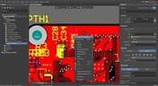
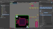
Designing for inspection is key to reliable manufacturing. This article covers practical PCB layout tips to optimize your board for AOI and X-ray inspection helping you reduce defects, false positives, and production delays.

Read More
Embedded thumbnail for How Close Can You Bring a Reference Plane?
How-To's • Jul 8, 2025
How Close Can You Bring a Reference Plane?

Explore our in-depth investigation into practical simulations using both Altium Designer and Polar Si9000. We demonstrate impedance sensitivity analysis and reveal the real limitations of optimizing reference plane proximity for improved signal shielding.

Start Watching
Blog • Jul 7, 2025
Understanding Systems Engineering

Read our brand-new article where we explore the key areas of an engineering project and the different stages of electronic product development from a project execution perspective. From initiation and planning to design, development, validation, testing, and certification, we walk you through each phase to help you understand how successful electronic products are brought to life.

Read More
Embedded thumbnail for Do PCB Thermal Vias Actually Work?
How-To's • Jul 3, 2025
Do PCB Thermal Vias Actually Work?

Are thermal vias really helping your PCB’s heat management? Tech Consultant Zach Peterson dives into simulation data, research, and a controversial article to uncover the truth. Learn why via count and spacing matter more than sheer quantity.

Start Watching
Blog • Jul 2, 2025
PCB First-Pass Yield: Small Decisions That Make a Big Difference

This article highlights how seemingly minor layout choices like trace spacing, component footprints, or stack-up details can dramatically impact whether a board passes fabrication and assembly the first time.

Read More
Blog • Jul 1, 2025
Implementing Design for Supply Chain Principles in Electronic Product Development

Designing with supply chain principles in mind helps you avoid delays, reduce costs, and ensure manufacturability. This article outlines practical strategies for component selection, sourcing, and lifecycle management to make your designs more resilient and production-ready.

Read More
Embedded thumbnail for Stripline Routing Deep Dive: How Close Is Too Close?
How-To's • Jun 30, 2025
Stripline Routing Deep Dive: How Close Is Too Close?

In this video, Zach Peterson takes a deep dive into what happens when reference layers are incorrectly set in a PCB stackup and how that affects impedance, signal integrity, and EMC. He also shares valuable insights into stripline routing proximity issues and best practices for assigning reference planes.

Start Watching
Blog • Jun 27, 2025
Beyond the BOM: How Proactive Component Selection Is Transforming Workflows

Learn how proactive component selection helps you avoid supply chain risks, reduce costs, and design more reliably. Our new article outlines key strategies and shows how tools like Altium 365 support smarter part decisions.

Read More
Blog • Jun 26, 2025
Power Integrity Issues?

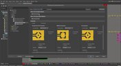
Power problems can be hard to spot until it’s too late. See how easy it is to analyze your power nets, check voltage drops, and improve reliability with Power Analyzer by Keysight - all without leaving your design environment.

Read More
Embedded thumbnail for Coming Soon: Solder Mask Zero Expansion
New in Altium Designer 25 • Jun 25, 2025
Coming Soon: Solder Mask Zero Expansion

Solder Mask Zero Expansion marks a move toward industry alignment, specifically with IPC-7351B and IPC-2581B standards. It changes the default solder mask expansion value from 4 mil to 0 mil. Discover more upcoming updates on our Coming Soon Page.

Start Watching
Blog • Jun 24, 2025
How to Design High-Speed PCBs Without Signal Surprises

Signal issues can sneak in early and cost you later. Read our whitepaper to see how Signal Analyzer by Keysight (inside Altium Designer) helps you catch problems fast and design with confidence.

Read More
Embedded thumbnail for Analog Supply without a Ferrite: Proper Isolation Techniques Explained
How-To's • Jun 20, 2025
Analog Supply without a Ferrite: Proper Isolation Techniques Explained

In our new tutorial, you'll learn why ferrite beads may not be the best choice for isolating analog and digital supply pins on integrated circuits. Zach Peterson debunks common misconceptions about ferrite bead isolation and introduces better alternatives, including dedicated LDOs, precision voltage references, and effective filtering techniques to help you achieve cleaner analog signals in your designs.

Start Watching
Blog • Jun 18, 2025
Beyond Basic Part Selection: Using Supply Chain Data to Validate Choices

Learn how to enhance part selection by using real-time supply chain data. This article shows how integrating insights like availability and lifecycle status helps you make smarter, risk-aware design choices.

Read More
Blog • Jun 17, 2025
Signal Mistakes Are Expensive

See how the Signal Analyzer by Keysight in Altium Designer lets you run signal integrity checks directly within your design environment. Read our article to learn how to effectively manage impedance, return paths, stackups, and more.

Read More
Embedded thumbnail for Enhanced Constraint Manager in Altium Designer 25. Part II: Physical Constraints and Routing Differential Pairs
Enhanced Constraint Manager in Altium Designer 25 • Jun 16, 2025
Enhanced Constraint Manager in Altium Designer 25. Part II: Physical Constraints and Routing Differential Pairs

In the second video of Samer Aldhaher’s "Enhanced Constraint Manager" series, we continue designing a 1 kW, 400 V brushless DC motor driver. This episode focuses on setting physical constraints using constraint sets, routing differential pairs, and demonstrating the Auto Shrinking feature in Altium Designer 25.

Start Watching
Embedded thumbnail for Auto-tuning Your Way to Faster PCB Design
Altium Designer's 25 Quantitative Benefits • Jun 13, 2025
Auto-tuning Your Way to Faster PCB Design

Watch how the Auto Tuning feature in Altium Designer 25 delivers optimized DDR4 routing in a single click! Fewer steps, massive time savings. Try our Benefit Calculator to estimate your own time and cost savings.

Start Watching
  • Show More
Tag (field_common_tag)
Blog • Mar 17, 2025
Cloud PCB Design: 5 Cloud Security Myths Debunked

This article addresses common misconceptions about cloud security in PCB design. It explains how modern cloud platforms, such as Altium 365, often provide superior security compared to traditional on-premises solutions. Key features like advanced infrastructure, granular access controls, and compliance with stringent regulations ensure the protection of valuable design data.

Read More
Blog • Mar 10, 2025
Renesas and Altium Announce Introduction of Renesas 365, Powered by Altium

Last week, Renesas Electronics and Altium proudly announced the introduction of Renesas 365, Powered by Altium—a first-of-its-kind industry solution designed to streamline electronic system development, from silicon selection to system lifecycle management. Renesas 365 will be demonstrated at Embedded World, Booth 5-371, from March 11-13 in Nuremberg, Germany.

Read More
Blog • Mar 6, 2025
DFM/DFA Requirements in Systems Engineering

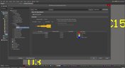
Learn how integrating DFM and DFA principles into systems engineering ensures manufacturable, cost-effective PCB designs by optimizing CAD, CAM, and requirements management in our new article by Javier Alcina.

Read More
Blog • Mar 4, 2025
Mastering EMI Control in PCB Design: Crosstalk Prevention for better EMI

Crosstalk control is essential for better EMI performance. Learn effective design techniques to reduce interference in the final installment of this series by Dario Fresu.

Read More
Blog • Mar 3, 2025
Best Practices for Electronics Project Management - Part 2

Part 2 of this series covers essential project management techniques for electronics design teams. Rafał Stępień discusses effective data organization, revision control, and collaboration strategies to improve efficiency and minimize errors.

Read More
Blog • Feb 27, 2025
Rigid-Flex PCBs: Understanding the Pros, Cons, and Fabrication Considerations

Read our new article which discusses the advantages of rigid-flex PCBs, such as space-saving designs and enhanced reliability, while also addressing potential challenges in their fabrication. It provides essential design and manufacturing tips to help engineers effectively implement this technology in various applications.

Read More
Blog • Feb 25, 2025
The Role of Automation & Robotics in Wire Harness Assembly

Our new article highlights how automation and robotics are transforming wire harness assembly, improving efficiency, precision, and cost-effectiveness. Technologies like robotic wire handling and AI-driven testing are paving the way for smarter production. However, challenges like custom designs and high costs still persist.

Read More
Blog • Feb 24, 2025
Best Practices for Electronics Project Management - Part 1

Check out the first part of "Best Practices for Electronics Project Management" by Rafał Stępień. It offers valuable advice on enhancing team communication and documentation in hardware design projects.

Read More
Blog • Feb 18, 2025
Wiring for the Final Frontier: A Guide to Space-Grade Harness Design

Wiring harnesses are mission-critical in space systems, requiring strict adherence to ECSS-Q-ST-70-61C and NASA-STD-8739.4A. In "Wiring for the Final Frontier: A Guide to Space-Grade Harness Design", Kamil Jasiński explores key design principles, material selection, and testing to ensure reliability in extreme environments.

Read More
Blog • Feb 11, 2025
The Future of Wire Harnesses in the Electric Vehicle and Electronics Era

Discover how wire harnesses are evolving to meet the demands of electric vehicles and modern electronics. Our latest article explores key trends like higher voltages, lightweight designs, and smart harnesses, along with challenges such as cost and supply chain issues.

Read More
Blog • Feb 10, 2025
Mastering EMI Control in PCB Design: Decoupling Strategies for PDN

Dario Fresu explores effective decoupling strategies for power distribution networks (PDNs) to minimize EMI in PCB designs. The article covers techniques like decoupling capacitors and power planes to ensure stable power delivery for integrated circuits.

Read More
Blog • Feb 4, 2025
Building Your Own Android Device with a Raspberry Pi

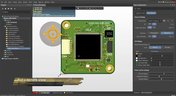
Learn how to turn a Raspberry Pi into a custom Android device. This guide covers hardware selection, software setup, and troubleshooting common issues.

Read More
Blog • Jan 31, 2025
How PCB Design Engineers Can Securely Share Design Files with External Teams

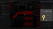
Learn how PCB design engineers can securely share design files with team members, clients, and manufacturers. Marek Orzeł explores best practices and tools to protect your intellectual property while ensuring efficient collaboration.

Read More
Blog • Jan 30, 2025
OEMs and Harness Manufacturers: Building Strong Collaboration for Success

Strong partnerships between OEMs and harness manufacturers are key to efficient, high-quality product development. In this article, Krishna Sundaram shows how collaboration, clear communication, and the right design tools can streamline the harness manufacturing process and drive success.

Read More
Blog • Jan 24, 2025
Ideal Rectifier Bridge

Read Marcin Lewandowski's article explaining how MOSFETs are replacing traditional diodes for reverse polarity protection. Step into the future of energy-efficient electronics!

Read More
Blog • Jan 21, 2025
Master Your Circuit Design: Dive into Worst Case Analysis

Dive into Worst Case Analysis techniques with Kamil Jasiński and ensure the reliability of your circuits. Master sensitivity analysis, Monte Carlo simulations, and more to confidently address real-world challenges.

Read More
  • Show More
Tag (field_common_tag)
Embedded thumbnail for Searching for Errors
• Jun 16, 2020
Searching for Errors

We’ve looked at how to set up the Design Rule Checker to help us analyze our PCB design errors. Now it’s time to resolve these errors and prep our design to start generating output files.

Start Watching
Embedded thumbnail for Performing Board DRC
• Jun 16, 2020
Performing Board DRC

Design rules are crucial to a PCB’s overall design and performance. It’s just as important to adhere to these rules and ensure that we didn’t overlook any unconnected nets or short circuits. This is why we need to run a Design Rule check.

Start Watching
Embedded thumbnail for Placing a Custom 3D Body in 3D View
• Jun 16, 2020
Placing a Custom 3D Body in 3D View

With the help of the 3D view, it is possible to view a PCB design from all sides, to check on component placement, silkscreen alignment, and many other visual aspects.

Start Watching
Embedded thumbnail for Silkscreen Placement
• Jun 16, 2020
Silkscreen Placement

The silkscreen layer is the layer on which we print any visual text or symbols on our PCB. With the help of this silkscreen layer, we can print our component designators, pin placement, and more.

Start Watching
Embedded thumbnail for Working with Polygon Pours
• Jun 16, 2020
Working with Polygon Pours

When working with common signals, the current levels are usually quite minimal, but when working with power nets it’s not uncommon to see current levels of a few amps. One of the reasons to use polygons is to maintain the quality and reliability of the power supply system.

Start Watching
Embedded thumbnail for Routing Post Processes
• Jun 16, 2020
Routing Post Processes

Depending on how you routed your board, it may be a time-consuming process to fix these manually. So we’ll dive into Route Glossing a little more, along with an automated way to retrace pre-existing routes.

Start Watching
Embedded thumbnail for PCB Layout Cleanup
• Jun 16, 2020
PCB Layout Cleanup

After the board has been routed, it’s almost certain that you’ll need to either move, delete, or adjust some traces. We’ll be looking at a few basic methods to easily modify and remove traces in our design.

Start Watching
Embedded thumbnail for Differential Pair Routing
• Jun 16, 2020
Differential Pair Routing

Routing Differential Pairs is similar to routing single traces, but there are additional rules and guidelines to follow that will help you avoid signal integrity problems.

Start Watching
Embedded thumbnail for Introduction to Routing
• Jun 16, 2020
Introduction to Routing

We’ve looked at different routing behaviors and options that we can change to make routing much easier. So we’re going to dive into the basics of routing and how these settings and routing modes can be applied.

Start Watching
Embedded thumbnail for Defining the Layer Stackup
• Jun 10, 2020
Defining the Layer Stackup

The PCB is designed and formed as a stack of layers and the definition of the PCB layer stack is a critical element of successful printed circuit board design. In Altium Designer, the Layer Stack Manager is used to develop the printed circuit board internal design including layer-pairing, careful via design, any back drilling requirements, rigid/flex requirements, copper balancing, layer stack symmetry, and material compliance. This video guides you through creation of a layer stackup, adding the necessary layers, as well as adding an impedance profile.

Start Watching
Embedded thumbnail for Searching for Errors in Schematic
• May 20, 2020
Searching for Errors in Schematic

Searching for Errors: Errors and mistakes happen to everyone - from beginners to professionals. So we always preach how it is paramount for your design to be validated before pushing it to the PCB. But luckily it’s pretty easy to find and analyze any errors using Altium Designer. We’ll take a look at how to find and analyze errors in your schematic.

Start Watching
Embedded thumbnail for Creating Net Classes
• Jun 2, 2020
Creating Net Classes

A Net Class is a collection of nets that can be used for creating a targeted design rule. So for example, you may want all power and ground nets to have a minimum track width to handle a specific current rating. So we’ll show you how to assign these nets to a NetClass. 

Start Watching
Embedded thumbnail for Configuring Design Rules - Part 2
• May 14, 2020
Configuring Design Rules - Part 2

Altium Designer uses the concept of Design Rules to define the requirements of a design. These rules collectively form an instruction set for the PCB Editor to follow. They cover every aspect of the design - from routing widths, clearances, plane connection styles and so on. With a well-defined set of design rules, you can successfully complete board designs with varying and often stringent design requirements.

Start Watching
Embedded thumbnail for Routing Modes and Setup
• May 12, 2020
Routing Modes and Setup

Most of you know that routing can be a time consuming process, but it doesn’t have to be a daunting task if you have the right tools. So we’ll be looking at what options and settings can help us perfect the art of routing.

Start Watching
Embedded thumbnail for PCB Component Placement
• May 12, 2020
PCB Component Placement

Component placement in the PCB is an important stage of the design process as it sets the precedent for efficient and clean routing. We’ll be diving into different component placement methods along with some tips and tricks that you can use to make this an easy process. 

Start Watching
Embedded thumbnail for Configuring the Basic Rules
• May 12, 2020
Configuring the Basic Rules

Altium Designer uses the concept of Design Rules to define the requirements of a design. These rules collectively form an instruction set for the PCB Editor to follow. They cover every aspect of the design - from routing widths, clearances, plane connection styles and so on. With a well-defined set of design rules, you can successfully complete board designs with varying and often stringent design requirements.

Start Watching
  • Show More
Tag (field_common_tag)
Ansys
On-Demand Webinar • Apr 7, 2024
A Seamless Connection Between ECAD and Simulation
Altium and Ansys have partnered to solve the most time-consuming steps in between and even further developed a seamless integration and structured approach.
Watch Now
Altium 365 PLM Integration Webinar Cover
On-Demand Webinar • Mar 29, 2024
Streamline Your Product Development - Altium 365 Cloud PLM Integration with Arena® PLM
Watch the webinar to discover how Altium 365 Cloud PLM Integration with Arena® can optimize your electronics product development processes. Discover the seamless connection between Altium 365 and the leading Cloud PLM system, designed to automate data flow, eliminate manual input, and minimize errors that lead to costly rework.
Watch Now
In-App Ad Cover GovCloud and AWS Webinar
On-Demand Webinar • Mar 18, 2024
Data Security and Access Controls for Electronics Development Teams
Watch the webinar that brings together the expertise of Altium 365 and AWS to introduce the specialized Altium 365 GovCloud within the robust AWS GovCloud infrastructure. This session is designed for IT and security professionals seeking advanced data protection and access control solutions for their electronics development teams.
Watch Now
Harness design
On-Demand Webinar • Mar 12, 2024
Unlock Complete System Design with Altium Designer 24
Join us in this webinar where you'll gain valuable insights into optimizing your design workflow, enhancing productivity, and overcoming common challenges faced in multi-board design projects.
Watch Now
Valispace Webinar Cover
On-Demand Webinar • Mar 8, 2024
Apply Modern Requirements and Systems Engineering for Faster Product Development
Watch the webinar to explore the future of electronics product development, focusing on Altium’s recent acquisition of Valispace. Understand how Valispace transforms requirements management and systems engineering, fostering enhanced collaboration, speeding up design processes, and leading to better products.
Watch Now
Agile Development Work for Hardware Webinar Cover
On-Demand Webinar • Feb 29, 2024
Can Agile Development Work for Hardware? 3 Critical Elements for Success
Watch the webinar to explore the benefits of agile methodologies and how they can be translated into the physical world of hardware development!
Watch Now
power analyzed on a pcb
On-Demand Webinar • Feb 26, 2024
Efficient Thermal Management with SPICE Simulation in Altium Designer 24
Uncover the art of predicting and refining circuit behavior using cutting-edge simulation tools within Altium Designer.
Watch Now
High speed
On-Demand Webinar • Feb 20, 2024
Advanced Techniques to design and optimize your High-Speed PCBs with Altium Designer
Watch Now
Pcb co design
On-Demand Webinar • Feb 20, 2024
PCB CoDesign in Altium Designer Demo
Watch Now
Harness design
On-Demand Webinar • Feb 20, 2024
Harness Design Demonstration
Discover how to streamline your cable harness design process using Altium's newest features—faster, simpler, and more integrated than ever before. Watch now and see how you can take your projects to the next level!
Watch Now
Ansys
On-Demand Webinar • Feb 20, 2024
Seamless Connection Between ECAD and Simulation Environment Using Ansys CoDesigner
Watch Now
PCB CoDesign Webinar
On-Demand Webinar • Jan 24, 2024
Discover How Altium Designer 24 Revolutionizes Team Dynamics in PCB Design
Expand your collaboration skills and stay ahead of the curve with PCB CoDesign. Design teams often grapple with prolonged design cycles and coordination issues, leading to delays and inefficiencies. In the current landscape, design processes are hindered by fragmented collaboration, resulting in increased layout times and difficulties in synchronizing design updates.
Watch Now
faster electronics design
On-Demand Webinar • Nov 30, 2023
Empowering Faster Electronics Development with Altium Designer 24
Revolutionize your approach to electronic product development and unlock the full potential of collaborative design. Join us as we discover how Altium Designer 24's intuitive and intelligent design platform empowers engineers and design teams to accomplish tasks with precision and speed, leading to enhanced efficiency and accelerated project timelines.
Watch Now
Gerber
On-Demand Webinar • Jul 20, 2020
From '0' to Gerber in 36.5 minutes
See how easy it is to create prototypes from scratch and automatically generate manufacturing files and standardized documentation using Altium Designer.
Watch Now
Tag (field_common_tag)
Loading
Loading...
Share link
Share with
Search by Update
Version
Update
25 26 24 23 22
25.0 25.1 25.2 25.3 25.4 25.5 25.6 25.7 25.8 25.9
26.1 26.2
24.10 24.9 24.8 24.7 24.6 24.5 24.4 24.3 24.2 24.1 24.0
23.11 23.10 23.9 23.8 23.7 23.6 23.5 23.4 23.3 23.2 23.1 23.0
22.11 22.10 22.9 22.8 22.7 22.6 22.5 22.4 22.3