
Main navigation

  • Home
  • Discover
  • Learning Center
  • What’s New

Second main navigation

  • Altium Community
  • Support
  • Documentation
×

Results

  • Updates
  • Blog 571
  • Video 541
  • Webinar 86
  • Playlist 53
Filters:
Tag (field_common_tag)
Blog • Jul 14, 2025
Material and Process Considerations That Influence Performance

Material and process choices play a key role in high-performance PCB design. This article highlights how stack-up configuration, substrate selection, and lamination strategy impact signal integrity, reliability, and manufacturability.

Read More
Embedded thumbnail for Compensating Transmission Line Losses in a PCB Calculator
How-To's • Jul 10, 2025
Compensating Transmission Line Losses in a PCB Calculator

This tutorial uncovers the key difference between ideal, lossless impedance calculations and real-world signal behavior giving you practical techniques to design controlled impedance PCBs that deliver reliable performance.

Start Watching
Blog • Jul 9, 2025
How to Make Your PCB Layout AOI and X-Ray Friendly

Designing for inspection is key to reliable manufacturing. This article covers practical PCB layout tips to optimize your board for AOI and X-ray inspection helping you reduce defects, false positives, and production delays.

Read More
Embedded thumbnail for How Close Can You Bring a Reference Plane?
How-To's • Jul 8, 2025
How Close Can You Bring a Reference Plane?

Explore our in-depth investigation into practical simulations using both Altium Designer and Polar Si9000. We demonstrate impedance sensitivity analysis and reveal the real limitations of optimizing reference plane proximity for improved signal shielding.

Start Watching
Blog • Jul 7, 2025
Understanding Systems Engineering

Read our brand-new article where we explore the key areas of an engineering project and the different stages of electronic product development from a project execution perspective. From initiation and planning to design, development, validation, testing, and certification, we walk you through each phase to help you understand how successful electronic products are brought to life.

Read More
Embedded thumbnail for Do PCB Thermal Vias Actually Work?
How-To's • Jul 3, 2025
Do PCB Thermal Vias Actually Work?

Are thermal vias really helping your PCB’s heat management? Tech Consultant Zach Peterson dives into simulation data, research, and a controversial article to uncover the truth. Learn why via count and spacing matter more than sheer quantity.

Start Watching
Blog • Jul 2, 2025
PCB First-Pass Yield: Small Decisions That Make a Big Difference

This article highlights how seemingly minor layout choices like trace spacing, component footprints, or stack-up details can dramatically impact whether a board passes fabrication and assembly the first time.

Read More
Blog • Jul 1, 2025
Implementing Design for Supply Chain Principles in Electronic Product Development

Designing with supply chain principles in mind helps you avoid delays, reduce costs, and ensure manufacturability. This article outlines practical strategies for component selection, sourcing, and lifecycle management to make your designs more resilient and production-ready.

Read More
Embedded thumbnail for Stripline Routing Deep Dive: How Close Is Too Close?
How-To's • Jun 30, 2025
Stripline Routing Deep Dive: How Close Is Too Close?

In this video, Zach Peterson takes a deep dive into what happens when reference layers are incorrectly set in a PCB stackup and how that affects impedance, signal integrity, and EMC. He also shares valuable insights into stripline routing proximity issues and best practices for assigning reference planes.

Start Watching
Blog • Jun 27, 2025
Beyond the BOM: How Proactive Component Selection Is Transforming Workflows

Learn how proactive component selection helps you avoid supply chain risks, reduce costs, and design more reliably. Our new article outlines key strategies and shows how tools like Altium 365 support smarter part decisions.

Read More
Blog • Jun 26, 2025
Power Integrity Issues?

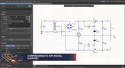
Power problems can be hard to spot until it’s too late. See how easy it is to analyze your power nets, check voltage drops, and improve reliability with Power Analyzer by Keysight - all without leaving your design environment.

Read More
Embedded thumbnail for Coming Soon: Solder Mask Zero Expansion
New in Altium Designer 25 • Jun 25, 2025
Coming Soon: Solder Mask Zero Expansion

Solder Mask Zero Expansion marks a move toward industry alignment, specifically with IPC-7351B and IPC-2581B standards. It changes the default solder mask expansion value from 4 mil to 0 mil. Discover more upcoming updates on our Coming Soon Page.

Start Watching
Blog • Jun 24, 2025
How to Design High-Speed PCBs Without Signal Surprises

Signal issues can sneak in early and cost you later. Read our whitepaper to see how Signal Analyzer by Keysight (inside Altium Designer) helps you catch problems fast and design with confidence.

Read More
Embedded thumbnail for Analog Supply without a Ferrite: Proper Isolation Techniques Explained
How-To's • Jun 20, 2025
Analog Supply without a Ferrite: Proper Isolation Techniques Explained

In our new tutorial, you'll learn why ferrite beads may not be the best choice for isolating analog and digital supply pins on integrated circuits. Zach Peterson debunks common misconceptions about ferrite bead isolation and introduces better alternatives, including dedicated LDOs, precision voltage references, and effective filtering techniques to help you achieve cleaner analog signals in your designs.

Start Watching
Blog • Jun 18, 2025
Beyond Basic Part Selection: Using Supply Chain Data to Validate Choices

Learn how to enhance part selection by using real-time supply chain data. This article shows how integrating insights like availability and lifecycle status helps you make smarter, risk-aware design choices.

Read More
Blog • Jun 17, 2025
Signal Mistakes Are Expensive

See how the Signal Analyzer by Keysight in Altium Designer lets you run signal integrity checks directly within your design environment. Read our article to learn how to effectively manage impedance, return paths, stackups, and more.

Read More
  • Show More
Tag (field_common_tag)
Article preview
Blog • Jul 15, 2020
Webinar "8 Reasons to Store Your Components in Altium 365"

Working with local libraries seems like a simple solution, but we often don’t take into account the added time spent maintaining libraries and sharing them between team members. This webinar showcases the advantages of component storage in Аltium 365 to resolve the issues of local libraries and component management.

Read More
Article preview
Blog • Jul 14, 2020
Bridging the Gap Between Designers and Customers

Every piece of electronic equipment starts with a great idea. Transforming great ideas into real, physical products takes a team of talented individuals and multiple companies coming together to make everything from the internal components to the external hardware. Paul Payen de la Garanderie, Founder and Owner of AW Audio, an engineering services company based in France, understands these challenges very well. With an extensive background in the Audio/Visual industry, Paul has had to work with multiple companies over the years, from small start-ups to celebrated AV firms.

Read More
Blog • Jul 9, 2020
Additive PCB Manufacturing: The Vaccine for Electronics Supply Shocks?

At this time, at least a quarter of the world’s population is under quarantine, with workers unable to go to offices or factories, leading to fundamental disabling of the world economy. The electronics industry is suffering greatly as well, dealing with a supply shock from factories shutting down in Southeast Asia, to demand-side shocks from Western markets literally shutting down. Now it is the electrical engineers taking the lead with additive PCB manufacturing.

Read More
Article preview
Blog • Jul 8, 2020
Webinar "6 Steps to Master Project Storage"

Altium 365 provides a secure cloud platform to store all of your design files in a single place so you can share them with anyone and access them from anywhere. This webinar discusses the advantages of placing, storing, and working with projects in Altium 365.

Read More
Article preview
Blog • Jul 7, 2020
Altium Designer 20 Changed My Layout Design Routines

I just finalized my first PCB design using Altium Designer 20. At the same time, I tested some new AD20 features, and in this article, I’ll share my thoughts about new layout design features which made the biggest impression for me: sliding, and any-angle routing.

Read More
Article preview
Blog • Jul 2, 2020
Designing for Antenna Isolation in Your Wireless System

Anyone who has taken apart an old cell phone or designs IoT devices knows multiple communication capabilities are present in these designs, each requiring different antennas. The RF designer should already take precautions for interconnect isolation, but antenna isolation is just as important when modeling and designing wireless systems.

Read More
Blog • Jun 30, 2020
PCB Trace and Pad Clearance: Low vs. High Voltage

High voltage/high current designs carry safety requirements which need to be met by designers. Similarly, high speed designs need to have suppressed crosstalk in order to ensure signal integrity. The key design aspects that relate to both areas are your PCB trace clearance and pad clearance values. These design choices are critical for balancing safety, noise suppression, and manufacturability.

Read More
Blog • Jun 25, 2020
Getting Through PCB DFM

In this article, we’ll discuss the key design features to implement, and steps to take prior to fabrication that will help prevent some DFM process pain.

Read More
Altium Designer Getting Started User Guide
Blog • Jun 23, 2020
Level Up Your Design Skills - Altium Designer Getting Started User Guide Update
We are happy to announce the new update of our Altium Designer Getting Started User Guide. Whether you are new to Altium Designer or you want to brush up on some topics, the Altium Designer Getting Started User Guide will take you from a beginner to a master in PCB design.  This is only the beginning! This guide will be updated with new information based on user feedback. Let’s first go over the contents of the guide.
Read More
Article preview
Blog • Jun 18, 2020
Modeling Copper Foil Roughness in Altium Designer's Impedance Profiler

With the new layer stack manager in Altium Designer®, you can now include copper foil roughness factors directly in your impedance calculator. This is quite easy to do in the layer stack manager, but it begs the question: what exactly is the copper roughness factor? Which value should be used for your interconnects?

Read More
Article preview
Blog • Jun 16, 2020
High-Speed Signal Routing: The 5 Important Constraints

After you capture your schematic as an initial layout and create an initial component arrangement, it’s time to define your routing constraints. Doing this early will allow your DRC engine to spot rules violations before you finish your layout. Likewise, you’ll be able to modify the default rule set to meet your layout requirements. Here are the important routing constraints you’ll need to check before you start routing your board.

Read More
Article preview
Blog • Jun 15, 2020
CoDesigner and MCAD Component Placement On-Demand Webinar

Learn how to place components from the MCAD side and synchronize them with Altium Designer ECAD models, designators, and sourcing data to simplify your design process.

Read More
Blog • Jun 11, 2020
How to Create a PCB Manufacturing Cost Estimation

Some manufacturers have very convenient PCB manufacturing cost estimation calculators you can use, but the real costs depend on a number of factors. If you’re an entrepreneur and you’re producing your own boards, or you are managing manufacturing, testing, and delivery for a new project, it’s your job to help clients understand the primary cost drivers for new boards. Here’s how you can get an estimate of your fabrication costs, both for local and overseas manufacturers.

Read More
Blog • Jun 9, 2020
PCB Mountable Connectors: SMD vs. Through-hole

Selecting a connector is as much an art as it is a science. The artistic side is all about aesthetics and satisfying clearances, while the scientific side is all about signal integrity. For PCB mountable connectors, you’ll need to choose between surface-mounted or through-hole connectors, and you’ll need to consider how each type affects signal integrity in your application. Here’s what you need to think about beyond the standard connector specifications.

Read More
Article preview
Blog • May 28, 2020
PCB Via Current-Carrying Capacity: How Hot is Too Hot?

Trace and via current-carrying capacity are legitimate design points to focus on when designing a new board that will carry high current. The goal is to keep conductor temperatures below some appropriate limit, which then helps keep components on the board cool.

Read More
Blog • May 21, 2020
How to Maximize Copper in Your PCB Design: The Pros and Cons of Copper Pouring Versus Placing

There is a saying in copper pour PCB design, “Copper is free.” It means a PCB editor designer must think in reverse. A board starts off as solid copper, and the copper you don’t want is removed. It is faster to build, less consumptive, and less expensive to make a board that is mostly copper as compared to the same size board that is mostly bare. Picking the correct technique will make the difference between an effortless or frustrating experience.

Read More
  • Show More
Tag (field_common_tag)
Embedded thumbnail for Insert Logo or Any Images on PCB
New in Altium Designer 21 • Dec 28, 2020
Insert Logo or Any Images on PCB

In the process of designing a printed circuit board, it becomes necessary to apply additional marking. It can be a company logo, interface designation or additional information signs. For ease of creating additional markings in Altium Designer 21, the PCB editor has a new Graphics tool that allows you to insert a picture into a specified area. This tool supports any of the four formats JPG, BMP, PNG, SVG. After selecting the image, it remains to specify its quality and the tool converts the image into a region on the active layer. If necessary, you can invert the image.

Start Watching
Embedded thumbnail for Using Polygons on Power Planes
New in Altium Designer 21 • Dec 28, 2020
Using Polygons on Power Planes

Traditionally, a PCB power plane is designed as a negative, that is, the objects placed on a power plane layer become voids in the copper when the board is fabricated. This approach is used because it is more efficient to generate the output data this way, as the bulk of a plane layer is normally copper; voids in the copper are only needed in specific locations such as around non-connected pads, or as separation voids when the plane is divided into different voltage regions.

Start Watching
Embedded thumbnail for Enhanced Polar Grid Support
New in Altium Designer 21 • Dec 28, 2020
Enhanced Polar Grid Support

Component placement is one of the main steps in board design. And in specific boards of a circular shape, it is convenient to use a polar grid for the location of components. Altium Designer 21 brings several improvements to the polar grid. Now, when a component is positioned in a polar grid, its properties additionally display location coordinates relative to this grid. Using them, you can quickly arrange the components in the right places. And moving the component off the grid, polar coordinates are automatically disabled.

Start Watching
Embedded thumbnail for New PCB Length Tuning Patterns
New in Altium Designer 21 • Dec 28, 2020
New PCB Length Tuning Patterns

Length matching is a critical element of high-speed design, usually solved by carefully tuning the lengths of critical routes. This release sees extensive improvements to both single-sided and differential pair length tuning capabilities. Length tuning now supports all three popular tuning patterns: Trombone, Sawtooth, and Accordion. If you are working with lower speed or lower frequency signals, you can get away with trombone tuning. For the Trombone patterns, the polygonal area that the pattern is constructed within can be thought of as a sleeve.

Start Watching
Embedded thumbnail for Expressions Library for Frequently Used Rules
New in Altium Designer 21 • Dec 28, 2020
Expressions Library for Frequently Used Rules

When working with design rules, we often use different scopes of the rules. To simplify the repetitive process of creating advanced type rules, the new Altium Designer 21 Rule Editor has the ability to save query-based object mapping scopes in a scoped library. To do this, it is enough to export the request by clicking on it with RMB. The library is presented through the Properties panel, where custom scopes can be edited, new ones added, and later reused in other custom constraint rules.

Start Watching
Embedded thumbnail for Constraint Rule Violations
New in Altium Designer 21 • Dec 28, 2020
Constraint Rule Violations

Enabled design constraint rules are applied to the current board design through a range of mechanisms, such as live Online Design Rule Checking, the batch Design Rule Checker or selectively run from the PCB Rules and Violations panel. Violations of those constraint Rules – where the specified and scoped limits are exceeded – are indicated through board graphics, panel entries and reports. With the introduction of a new Rules Editor in Altium Designer 21, violations of these rules are now displayed in the Rules Editor itself.

Start Watching
Embedded thumbnail for Table-based Approach for Design Rules and Constraints
New in Altium Designer 21 • Dec 28, 2020
Table-based Approach for Design Rules and Constraints

Define and assign a specific list of rules and constraints to all critical design elements, such as components, nets, and LVDS.

Start Watching
Embedded thumbnail for Comprehensive Simulation Model Support
New in Altium Designer 21 • Dec 28, 2020
Comprehensive Simulation Model Support

Having accurate SPICE models is critical to the success of your simulation. Altium Designer now supports analog PSpice, LTspice, and more including generic component SPICE models for when you can’t find company models. Generic components contain Spice model parameters to simplify simulation. When you are done with simulation, quickly replace your generic components with an existing component to finish your design.

Start Watching
Embedded thumbnail for Easy to Start Simulations
New in Altium Designer 21 • Dec 28, 2020
Easy to Start Simulations

0:00 Simulation Dashboard Panel Following on from the recent introduction of an advanced new SPICE Simulation engine for Altium Designer, the latest round of Simulation updates focuses on user interface. A major component of the Altium Designer Simulation user interface updates is the introduction of the Simulation Dashboard panel. The panel offers a greatly simplified approach to checking, configuring, running and reviewing simulations.

Start Watching
Embedded thumbnail for Rigid-Flex Board Planning Mode
New in Altium Designer 21 • Dec 28, 2020
Rigid-Flex Board Planning Mode

This new release of Altium Designer 21 includes significant improvements to the Rigid-Flex board designs. Along with many bug fixes and enhancements, the next phase of Altium Rigid-Flex technology development is providing functional improvements. It is now possible to create new board regions by primitives using the appropriate command from the Design » Board Shape menu. The properties of all created regions are now displayed in the Properties panel where you can edit the name of each region and define the previously created stacks for each region of the board.

Start Watching
Embedded thumbnail for Component Pin to Multiple Pad Mapping
New in Altium Designer 21 • Dec 28, 2020
Component Pin to Multiple Pad Mapping

This release introduces flexible pin to pad mapping capabilities for managed components. Enhancements to the Single Component Editor and the introduction of a new Pins panel allow component symbol pins to be mapped to any component footprint pad, or any number of footprint pads. The Pins panel, opened from the editor's button, allows the default one-to-one pin-pad mapping to be changed to a custom relationship, such as one pin being connected to multiple footprint pads – or any other non-aligned pin to pad number relationship.

Start Watching
Embedded thumbnail for Enhanced Navigation by Nets in Schematic - Altium Designer 21 What's New
New in Altium Designer 21 • Dec 28, 2020
Enhanced Navigation by Nets in Schematic - Altium Designer 21 What's New

Altium Designer 21 brings many improvements to the schematic editor aimed at visualizing circuits and improving navigation through them in multi-sheet and hierarchical designs. By holding Alt and clicking on the net, All schematic instances of the net are highlighted, while other objects are dimmed, to visibly indicate the signal/power propagation in the design using one simple action. The changes also affected the Identification of net names. Now logical and physical names of a net are displayed in the properties panel as well as when you hover over this wire.

Start Watching
Embedded thumbnail for Intelligent Schematic Insights
New in Altium Designer 21 • Dec 28, 2020
Intelligent Schematic Insights

Due to advances in the format and compilation of the Altium Designer data model, schematic Wire objects have now evolved from a simple graphical object to a more advanced form that can be directly associated with electrical parameters. As a result, the Wire mode of the Properties panel has been updated to provide an expanded set of options and a wider range of information. The new additions include a General section for net parameter options and information, and a Parameters section that lists the User Parameters, Rules and Net Classes associated with the Wire's assigned net.

Start Watching
Embedded thumbnail for Start Your Schematic with Generic Components
New in Altium Designer 21 • Dec 28, 2020
Start Your Schematic with Generic Components

It can be challenging to pick the right components when working on a new schematic. You have to consider availability, cost, and various parametric requirements. What if you could place a component to complete your design and quickly replace it when you are ready for layout? Introducing new Generic Components. Simply provide generic parameters, such as Value or Footprint, to greatly speed-up your capturing process while eliminating the need to search for specific Part Numbers or creating a needed component from scratch.

Start Watching
Embedded thumbnail for MCAD CoDesigner Overview
Working with MCAD CoDesigner extension • Dec 21, 2020
MCAD CoDesigner Overview

The MCAD CoDesigner in Altium Designer allows for seamless design transfer between the Electrical and Mechanical designers. In this overview, we’ll show you how to transfer from Altium Designer to your CAD tool of choice, then how to resize the board, add mounting holes, add a new connector, and update the board design in Altium Designer.

Start Watching
Embedded thumbnail for Bringing an MCAD Enclosure to ECAD
Working with MCAD CoDesigner extension • Nov 16, 2020
Bringing an MCAD Enclosure to ECAD

The Altium Designer MCAD CoDesigner panel and extension make it easy to move a 3D enclosure model from your MCAD tool to Altium Designer. We'll show you how and what to watch out for while your transferring your enclosure model to Altium Designer.

Start Watching
  • Show More
Tag (field_common_tag)
Ansys
On-Demand Webinar • Apr 7, 2024
A Seamless Connection Between ECAD and Simulation
Altium and Ansys have partnered to solve the most time-consuming steps in between and even further developed a seamless integration and structured approach.
Watch Now
Altium 365 PLM Integration Webinar Cover
On-Demand Webinar • Mar 29, 2024
Streamline Your Product Development - Altium 365 Cloud PLM Integration with Arena® PLM
Watch the webinar to discover how Altium 365 Cloud PLM Integration with Arena® can optimize your electronics product development processes. Discover the seamless connection between Altium 365 and the leading Cloud PLM system, designed to automate data flow, eliminate manual input, and minimize errors that lead to costly rework.
Watch Now
In-App Ad Cover GovCloud and AWS Webinar
On-Demand Webinar • Mar 18, 2024
Data Security and Access Controls for Electronics Development Teams
Watch the webinar that brings together the expertise of Altium 365 and AWS to introduce the specialized Altium 365 GovCloud within the robust AWS GovCloud infrastructure. This session is designed for IT and security professionals seeking advanced data protection and access control solutions for their electronics development teams.
Watch Now
Harness design
On-Demand Webinar • Mar 12, 2024
Unlock Complete System Design with Altium Designer 24
Join us in this webinar where you'll gain valuable insights into optimizing your design workflow, enhancing productivity, and overcoming common challenges faced in multi-board design projects.
Watch Now
Valispace Webinar Cover
On-Demand Webinar • Mar 8, 2024
Apply Modern Requirements and Systems Engineering for Faster Product Development
Watch the webinar to explore the future of electronics product development, focusing on Altium’s recent acquisition of Valispace. Understand how Valispace transforms requirements management and systems engineering, fostering enhanced collaboration, speeding up design processes, and leading to better products.
Watch Now
Agile Development Work for Hardware Webinar Cover
On-Demand Webinar • Feb 29, 2024
Can Agile Development Work for Hardware? 3 Critical Elements for Success
Watch the webinar to explore the benefits of agile methodologies and how they can be translated into the physical world of hardware development!
Watch Now
power analyzed on a pcb
On-Demand Webinar • Feb 26, 2024
Efficient Thermal Management with SPICE Simulation in Altium Designer 24
Uncover the art of predicting and refining circuit behavior using cutting-edge simulation tools within Altium Designer.
Watch Now
High speed
On-Demand Webinar • Feb 20, 2024
Advanced Techniques to design and optimize your High-Speed PCBs with Altium Designer
Watch Now
Pcb co design
On-Demand Webinar • Feb 20, 2024
PCB CoDesign in Altium Designer Demo
Watch Now
Harness design
On-Demand Webinar • Feb 20, 2024
Harness Design Demonstration
Discover how to streamline your cable harness design process using Altium's newest features—faster, simpler, and more integrated than ever before. Watch now and see how you can take your projects to the next level!
Watch Now
Ansys
On-Demand Webinar • Feb 20, 2024
Seamless Connection Between ECAD and Simulation Environment Using Ansys CoDesigner
Watch Now
PCB CoDesign Webinar
On-Demand Webinar • Jan 24, 2024
Discover How Altium Designer 24 Revolutionizes Team Dynamics in PCB Design
Expand your collaboration skills and stay ahead of the curve with PCB CoDesign. Design teams often grapple with prolonged design cycles and coordination issues, leading to delays and inefficiencies. In the current landscape, design processes are hindered by fragmented collaboration, resulting in increased layout times and difficulties in synchronizing design updates.
Watch Now
faster electronics design
On-Demand Webinar • Nov 30, 2023
Empowering Faster Electronics Development with Altium Designer 24
Revolutionize your approach to electronic product development and unlock the full potential of collaborative design. Join us as we discover how Altium Designer 24's intuitive and intelligent design platform empowers engineers and design teams to accomplish tasks with precision and speed, leading to enhanced efficiency and accelerated project timelines.
Watch Now
Gerber
On-Demand Webinar • Jul 20, 2020
From '0' to Gerber in 36.5 minutes
See how easy it is to create prototypes from scratch and automatically generate manufacturing files and standardized documentation using Altium Designer.
Watch Now
Tag (field_common_tag)
Loading
Loading...
Share link
Share with
Search by Update
Version
Update
25 26 24 23 22
25.0 25.1 25.2 25.3 25.4 25.5 25.6 25.7 25.8 25.9
26.1 26.2
24.10 24.9 24.8 24.7 24.6 24.5 24.4 24.3 24.2 24.1 24.0
23.11 23.10 23.9 23.8 23.7 23.6 23.5 23.4 23.3 23.2 23.1 23.0
22.11 22.10 22.9 22.8 22.7 22.6 22.5 22.4 22.3