
Main navigation

  • Home
  • Discover
  • Learning Center
  • What’s New

Second main navigation

  • Altium Community
  • Support
  • Documentation
×

Results

  • Updates
  • Blog 570
  • Video 539
  • Webinar 86
  • Playlist 53
Filters:
Tag (field_common_tag)
Embedded thumbnail for How Close Can You Bring a Reference Plane?
How-To's • Jul 8, 2025
How Close Can You Bring a Reference Plane?

Explore our in-depth investigation into practical simulations using both Altium Designer and Polar Si9000. We demonstrate impedance sensitivity analysis and reveal the real limitations of optimizing reference plane proximity for improved signal shielding.

Start Watching
Blog • Jul 7, 2025
Understanding Systems Engineering

Read our brand-new article where we explore the key areas of an engineering project and the different stages of electronic product development from a project execution perspective. From initiation and planning to design, development, validation, testing, and certification, we walk you through each phase to help you understand how successful electronic products are brought to life.

Read More
Embedded thumbnail for Do PCB Thermal Vias Actually Work?
How-To's • Jul 3, 2025
Do PCB Thermal Vias Actually Work?

Are thermal vias really helping your PCB’s heat management? Tech Consultant Zach Peterson dives into simulation data, research, and a controversial article to uncover the truth. Learn why via count and spacing matter more than sheer quantity.

Start Watching
Blog • Jul 2, 2025
PCB First-Pass Yield: Small Decisions That Make a Big Difference

This article highlights how seemingly minor layout choices like trace spacing, component footprints, or stack-up details can dramatically impact whether a board passes fabrication and assembly the first time.

Read More
Blog • Jul 1, 2025
Implementing Design for Supply Chain Principles in Electronic Product Development

Designing with supply chain principles in mind helps you avoid delays, reduce costs, and ensure manufacturability. This article outlines practical strategies for component selection, sourcing, and lifecycle management to make your designs more resilient and production-ready.

Read More
Embedded thumbnail for Stripline Routing Deep Dive: How Close Is Too Close?
How-To's • Jun 30, 2025
Stripline Routing Deep Dive: How Close Is Too Close?

In this video, Zach Peterson takes a deep dive into what happens when reference layers are incorrectly set in a PCB stackup and how that affects impedance, signal integrity, and EMC. He also shares valuable insights into stripline routing proximity issues and best practices for assigning reference planes.

Start Watching
Blog • Jun 27, 2025
Beyond the BOM: How Proactive Component Selection Is Transforming Workflows

Learn how proactive component selection helps you avoid supply chain risks, reduce costs, and design more reliably. Our new article outlines key strategies and shows how tools like Altium 365 support smarter part decisions.

Read More
Blog • Jun 26, 2025
Power Integrity Issues?

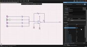
Power problems can be hard to spot until it’s too late. See how easy it is to analyze your power nets, check voltage drops, and improve reliability with Power Analyzer by Keysight - all without leaving your design environment.

Read More
Embedded thumbnail for Coming Soon: Solder Mask Zero Expansion
New in Altium Designer 25 • Jun 25, 2025
Coming Soon: Solder Mask Zero Expansion

Solder Mask Zero Expansion marks a move toward industry alignment, specifically with IPC-7351B and IPC-2581B standards. It changes the default solder mask expansion value from 4 mil to 0 mil. Discover more upcoming updates on our Coming Soon Page.

Start Watching
Blog • Jun 24, 2025
How to Design High-Speed PCBs Without Signal Surprises

Signal issues can sneak in early and cost you later. Read our whitepaper to see how Signal Analyzer by Keysight (inside Altium Designer) helps you catch problems fast and design with confidence.

Read More
Embedded thumbnail for Analog Supply without a Ferrite: Proper Isolation Techniques Explained
How-To's • Jun 20, 2025
Analog Supply without a Ferrite: Proper Isolation Techniques Explained

In our new tutorial, you'll learn why ferrite beads may not be the best choice for isolating analog and digital supply pins on integrated circuits. Zach Peterson debunks common misconceptions about ferrite bead isolation and introduces better alternatives, including dedicated LDOs, precision voltage references, and effective filtering techniques to help you achieve cleaner analog signals in your designs.

Start Watching
Blog • Jun 18, 2025
Beyond Basic Part Selection: Using Supply Chain Data to Validate Choices

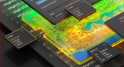
Learn how to enhance part selection by using real-time supply chain data. This article shows how integrating insights like availability and lifecycle status helps you make smarter, risk-aware design choices.

Read More
Blog • Jun 17, 2025
Signal Mistakes Are Expensive

See how the Signal Analyzer by Keysight in Altium Designer lets you run signal integrity checks directly within your design environment. Read our article to learn how to effectively manage impedance, return paths, stackups, and more.

Read More
Embedded thumbnail for Enhanced Constraint Manager in Altium Designer 25. Part II: Physical Constraints and Routing Differential Pairs
Enhanced Constraint Manager in Altium Designer 25 • Jun 16, 2025
Enhanced Constraint Manager in Altium Designer 25. Part II: Physical Constraints and Routing Differential Pairs

In the second video of Samer Aldhaher’s "Enhanced Constraint Manager" series, we continue designing a 1 kW, 400 V brushless DC motor driver. This episode focuses on setting physical constraints using constraint sets, routing differential pairs, and demonstrating the Auto Shrinking feature in Altium Designer 25.

Start Watching
Embedded thumbnail for Auto-tuning Your Way to Faster PCB Design
Altium Designer's 25 Quantitative Benefits • Jun 13, 2025
Auto-tuning Your Way to Faster PCB Design

Watch how the Auto Tuning feature in Altium Designer 25 delivers optimized DDR4 routing in a single click! Fewer steps, massive time savings. Try our Benefit Calculator to estimate your own time and cost savings.

Start Watching
Blog • Jun 12, 2025
Twice the Insight. One Seamless Simulation Bundle

Ensure power and signal integrity with the Keysight Bundle in Altium Designer. Catch issues early, reduce rework, and optimize your PCBs - all within one integrated environment featuring Signal & Power Analyzer.

Read More
  • Show More
Tag (field_common_tag)
Why Use a Version Control System in PCB Design
Blog • Dec 17, 2021
Why Use a Version Control System in PCB Design

Version Control Systems (VCS) have been around for many decades within the software world but can be surprisingly new to some folks in the electronics design industry. This article will cover what a VCS is, what it does, and why you should be using one for your PCB design projects.

Read More
IPC 6012 Class 3 Annular Ring
Blog • Dec 16, 2021
Meeting Standards: IPC 6012 Class 3 Annular Ring

Designers often conflate leftover annular ring and pad sizes - they need to place a sufficiently large pad size on the surface layer to ensure that the annular ring that is leftover during fabrication will be large enough. As long as the annular ring is sufficiently large, the drill hit will not be considered defective and the board will have passed inspection. In this article, I'll discuss the limits on IPC-6012 Class 3 annular rings as these are a standard fabrication requirement for high-reliability rigid PCBs.

Read More
PCB fabrication notes
Blog • Dec 14, 2021
Decoding PCB Fabrication Notes

Sending a board out for fabrication is an exciting and nerve-wracking moment. Why not just give your fabricator your design files and let them figure it out? There are a few reasons for this, but it means the responsibility comes back to you as the designer to produce manufacturing files and documentation for your PCB. It’s actually quite simple if you have the right design tools. We’ll look at how you can do this inside your PCB layout and how this will help you quickly generate data for your manufacturer.

Read More
HDI PCB design and HDI PCB manufacturing process
Blog • Dec 9, 2021
Design Basics for HDI and the HDI PCB Manufacturing Process

As the world of technology has evolved, so has the need to pack more capabilities into smaller packages. PCBs designed using high-density interconnect techniques tend to be smaller as more components are packed in a smaller space. An HDI PCB uses blind, buried, and micro vias, vias in pads, and very thin traces to pack more components into a smaller area. We’ll show you the design basics for HDI and how Altium Designer® can help you create a powerful HDI PCB.

Read More
All About PCB Test Points
Blog • Dec 7, 2021
Is It Printed or a Component? All About PCB Test Points

Test points in your electronic assembly will give you a location to access components and take important measurements to verify functionality. If you’ve never used a test point or you’re not sure if you need test points, keep reading to see what options you have for test point usage in your PCB layout.

Read More
How to Design to a Differential Impedance Specification
Blog • Dec 2, 2021
How to Design to a Differential Impedance Specification

The concept and implementation of differential impedance are both sometimes misunderstood. In addition, the design of a channel to reach a specific differential impedance is often done in a haphazard way. The very concept of differential impedance is something of a mathematical construct that doesn’t fully capture the behavior of each signal in a differential trace. Keep reading to see a bit more depth on how to design to a differential impedance spec and exactly what it means for your design.

Read More
Draftsman Drawing
Blog • Nov 30, 2021
The Main Advantages when using Draftsman to Create a Component Mounting Drawing

Quite often, a standard assembly drawing is not enough to ensure the quality of a PCB assembly, especially when designing high-density boards. It would also be helpful to include additional detailing for simpler devices. The use of a Draftsman document brings an elegant, yet powerful solution to make these tasks easier.

Read More
Product Lifecycle Management in Electronics Manufacturing
Blog • Nov 25, 2021
Product Lifecycle Management in Electronics Manufacturing

An effective product lifecycle management (PLM) solution will integrate the tools and processes employed to design, develop and manufacture a new device. This solution goes beyond engineering activities to include the project management, process control, and financial management of the end-to-end business processes. PLM solutions create this collaborative environment where product development can flourish, bringing additional benefits in efficiencies and transparent communications, breaking silos, and speeding up the development process.

Read More
Tight versus loose coupling
Blog • Nov 23, 2021
Should You Use Tight vs. Loose Differential Pair Spacing and Coupling?

In this article, we want to get closer to a realistic description of tight coupling vs. loose coupling in terms of differential pair spacing, as well as how the differential pair spacing affects things like impedance, differential-mode noise, reception of common-mode noise, and termination. As we’ll see, the focus on tight coupling has its merits, but it’s often cited as necessary for the wrong reasons.

Read More
Engineering Design Review Guide
Blog • Nov 18, 2021
How to Solve Your Engineering Design Review Challenges

You’ve possibly gone through plenty of engineering design reviews, both on the front-end of a project and the back-end before manufacturing. Engineering design reviews are performed to accomplish multiple objectives, and with many engineering teams taking a systems-based approach to design and production, electronics design teams will need to review much more than just a PCB layout and BOM. Today’s challenges with sourcing, manufacturability, reliability, and mechanical constraints are all areas that must be confronted in real designs

Read More
Schematic Review Checklist
Blog • Nov 16, 2021
Schematic Review Checklist

One of the most common points of failure of a device occurs even before you start to layout your circuit board. Mistakes in your schematic design can easily make their way all the way into prototypes or production without a second thought once layout starts. In this article, I’m not going to extol the virtues of a good schematic design. Instead, this article is a simple no frills checklist.

Read More
Via current carrying capacity for PCBs
Blog • Nov 11, 2021
PCB Via Current-Carrying Capacity: How Hot is Too Hot?

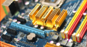
One common question from designers is current-carrying capacity of conductors in a PCB. Trace and via current-carrying capacity are legitimate design points to focus on when designing a new board that will carry high current. The goal is to keep conductor temperatures below some appropriate limit, which then helps keep components on the board cool. Let’s dig into the current state of thermal demands on vias in PCBs and how they compare to internal and external PCB traces.

Read More
PCB Shield
Blog • Nov 9, 2021
Phalanx, not Failure: PCB Shielding to Protect Your Design

A combination of good printed circuit board design and good shielding mitigates EMI. Good PCB design for EMI shielding revolves around the layout, the placement of filters, and ground planes. A well-designed PCB minimizes parasitic capacitance and ground loops. Keep reading to learn more about PCB shielding.

Read More
Man working in Altium Designer
Blog • Nov 4, 2021
Best Practices in Hardware Version Control Systems

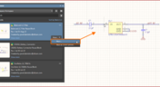
Any project can get very complex, and the PCB design team needs to track revisions throughout a project. Why worry about tracking revisions? In the event you ever receive changes to product functional requirements, major changes are made to your product’s architecture, or you’re ready to finalize the design and prepare for fabrication, it’s best to clone a project at its current state and begin working on a new version. Keeping track of all these design changes in a PCB design project takes the type of hardware version control tools you’ll find in Altium 365™.

Read More
Copper pour and via stitching
Blog • Oct 28, 2021
Copper Pour and Via Stitching: Do You Need Them in a PCB Layout?

To pour or not to pour, to stitch or not to stitch… Over many years, some common “rules of thumb” have become very popular and, ultimately, taken a bit out of context. Rules of thumb are not always wrong, but taking PCB design recommendations out of context helps justify bad design practices, and it can even affect the producibility of your board. Like many aspects of a physical PCB layout, via stitching and copper pour can be like acid: quite useful if implemented properly, but also dangerous if used indiscriminately.

Read More
MOSFET Components
Blog • Oct 26, 2021
Should You Use Power MOSFETs in Series?

Power MOSFETs enable a huge range of electronic systems, specifically in situations where BJTs are not useful or efficient. MOSFETs can be used in high current systems in parallel arrangements, but what about their use in series? Both arrangements of MOSFETs have their pitfalls that designers should consider. Let’s look at MOSFETs in series as they are quite useful in certain systems, but be careful to design your circuits and your PCB for reliability.

Read More
  • Show More
Tag (field_common_tag)
Embedded thumbnail for Buck Converter
Simulation in Altium Designer • Sep 25, 2023
Buck Converter

Learn how to run a transient simulation, analyze the waveforms, and measurement techniques you can use to determine a voltage ripple with a buck converter as an example. 

Start Watching
Embedded thumbnail for Edge Plating in RF Design
How-To's • Sep 21, 2023
Edge Plating in RF Design

PCB Edge Plating provides additional noise suppression and improves EMC. In this video we provide you some practical tips for creating metalized PCB edges in Altium Designer.

Start Watching
Embedded thumbnail for Custom Paste Mask and Solder Mask
Custom Pad Stack in Altium Designer • Sep 19, 2023
Custom Paste Mask and Solder Mask

Altium Designer allows you to freely customize paste and solder mask shapes, which allows you to adapt your design for non-standard component footprints.

Start Watching
Embedded thumbnail for Colpitts Oscillator
Simulation in Altium Designer • Sep 15, 2023
Colpitts Oscillator

Learn how to effectively fix errors in circuit simulation and other problem-solving techniques using a Colpitts Oscillator design as an example. 

Start Watching
Embedded thumbnail for Custom Thermal Reliefs for Pads
Custom Pad Stack in Altium Designer • Sep 12, 2023
Custom Thermal Reliefs for Pads

Altium Designer allows you to add, remove, and edit thermal relief spikes anywhere on a pad, regardless of its shape. Using these can improve soldering and prevent manufacturing problems like tombstoning.

Start Watching
Embedded thumbnail for Notch Filter
Simulation in Altium Designer • Sep 8, 2023
Notch Filter

Learn how to run an AC sweep analysis, execute a Monte Carlo simulation, and interpret the results using a notch filter as an example. 

Start Watching
Embedded thumbnail for Custom Pad Shapes
Custom Pad Stack in Altium Designer • Sep 5, 2023
Custom Pad Shapes

Modern components often contain pads with complex shapes. Altium Designer allows you to create custom pad shapes quickly and easily, and manage them like you would a standard pad.

Start Watching
Embedded thumbnail for Low-Pass Filter
Simulation in Altium Designer • Aug 30, 2023
Low-Pass Filter

Learn how to modify an op amp low-pass filter circuit for simulation. 

Start Watching
Embedded thumbnail for Design Reuse
How-To's • Aug 29, 2023
Design Reuse

If you need to shorten your time-to-market, reduce costs, and minimize errors in the design process. Then you need to make sure that you’re designing smarter, with design reuse blocks. Check out this demo to see how it works.

Start Watching
Embedded thumbnail for Flyback Converter
Simulation in Altium Designer • Aug 25, 2023
Flyback Converter

Learn how to use transient analysis on an example flyback converter and handle basic errors during the simulation preparation. 

Start Watching
Embedded thumbnail for Analog to Digital Converter
Simulation in Altium Designer • Aug 21, 2023
Analog to Digital Converter

Learn how to run a mixed-signal (analog and digital) design simulation.

Start Watching
Embedded thumbnail for Back Drilling in Altium Designer
How-To's • Aug 18, 2023
Back Drilling in Altium Designer

In this video, we will learn about Back Drilling technology, how to set up back drilling using the Layer Stack Manager, and how to set up the Stub Length sizes for back drilling by specifying applicable nets using the Design Rules Editor.

Start Watching
Embedded thumbnail for Distributed - Element Circuits in RF Design
How-To's • Aug 16, 2023
Distributed - Element Circuits in RF Design

The capacitance and inductance of Distributed-Element circuits are determined by the shape and location of different copper elements in the PCB layout, instead of being concentrated in one point in space. Learn how to work with these circuits in Altium Designer.

Start Watching
Embedded thumbnail for Collaborative Editing
How-To's • Aug 10, 2023
Collaborative Editing

Save time and minimize reworks while teaming up on a PCB design from anywhere in the world. Watch the video for a sneak preview of the new collaborative editing functionality.

Start Watching
Embedded thumbnail for Exporting Results
How To Work with Power Analyzer by Keysight • Aug 8, 2023
Exporting Results

After completing your simulation in Power Analyzer by Keysight, you will likely need to export some of the results for further analysis. In this video, we will show you how to prepare a report once the simulation is done.

Start Watching
Embedded thumbnail for Plane Connect - Direct in RF Design
How-To's • Aug 3, 2023
Plane Connect - Direct in RF Design

Designing high-frequency circuit boards requires a sharp eye toward maintaining signal integrity. Some signal connections are more prone to interruption than others. In this video, you can learn how Altium Designer's Polygon Connect Design Rule and the Thermal Relief option can help in the PCB design process.

Start Watching
  • Show More
Tag (field_common_tag)
ADv25
On-Demand Webinar • Oct 24, 2024
Modernizing Engineering Workflows: Altium Designer 25 and the Future of Concurrent Design
Struggling with team misalignment and design errors? Join our exciting webinar to discover the groundbreaking advancements in Altium Designer 25!
Watch Now
KiCad Webinar
On-Demand Webinar • Oct 16, 2024
Taking the Next Step: Growing Beyond KiCad with Altium
Join our upcoming webinar to discover how Altium Designer can transition your KiCad projects without any data loss
Watch Now
Synchronize to Optimize Jira Integration
On-Demand Webinar • Oct 7, 2024
Synchronize to Optimize: Enhancing Efficiency with Jira Integration for Altium 365
Tired of juggling multiple tools for project management? Watch the webinar and see how Jira Integration for Altium 365 can optimize your workflows.
Watch Now
Wire bonding
On-Demand Webinar • Sep 29, 2024
Unlock New Design Possibilities with Wire Bonding
Explore how wire bonding can enhance your designs, provide size reduction, improve power management, and increase mechanical reliability.
Watch Now
routing
On-Demand Webinar • Sep 29, 2024
Advanced Routing Features & Techniques
To help you get the most out of your experience with Altium Designer, join our webinar this month and learn advanced routing techniques.
Watch Now
signal analyzer
On-Demand Webinar • Sep 25, 2024
Signal Integrity Made Simple
Discover how to easily detect and resolve high-speed signal integrity challenges without the need for extensive expertise.
Watch Now
competitive-displacement-webinar-3
On-Demand Webinar • Sep 20, 2024
Mastering Design Complexity: How Altium Designer Outperforms Cadence in Solving Workflow and Engineering Challenges - Part 2
Join our webinar to learn how to enhance efficiency, foster better collaboration, and accelerate your time-to-market with Altium unified solutions.
Watch Now
Breaking Down Silos Webinar
On-Demand Webinar • Sep 16, 2024
Breaking Down Data Silos: A Practical Comparison of Altium and Cadence in Cross-Functional PCB Design
Join us for a webinar that addresses the critical challenges of maintaining design data continuity across various design functions.
Watch Now
Draftsman
On-Demand Webinar • Sep 10, 2024
Mastering Design Complexity: How Altium Designer Outperforms Cadence in Solving Workflow and Engineering Challenges
Join our upcoming webinar to discover why engineers consistently choose Altium Designer as the standard in PCB design.
Watch Now
SPICE
On-Demand Webinar • Sep 3, 2024
Mastering SPICE Simulation in Altium Designer
Discover how the SPICE engine in Altium Designer can help you easily verify that your finished project functions as intended.
Watch Now
Output job
On-Demand Webinar • Aug 24, 2024
Beyond PCB Design with Altium Designer
In this webinar we'll dive into the essential aspects that go beyond the schematic and layout.
Watch Now
PCB
On-Demand Webinar • Aug 23, 2024
Elevate Your Design Skills: Tips & Tricks for Success
Discover practical insights and efficient methods that can enhance your PCB design capabilities.
Watch Now
Cyber Security Webinar Cover
On-Demand Webinar • Aug 6, 2024
The Anatomy of IT Compliance in Electronics Development: Altium 365 & AWS GovCloud
Are you an IT or security professional looking for a secure electronics design collaboration platform that could also support your ITAR and EAR compliance efforts? If so, watch this webinar to bring together the expertise of Altium 365 and AWS!
Watch Now
Design reuse
On-Demand Webinar • Aug 1, 2024
How to Speed-up Product Development with Reusable Circuitry
In this webinar you'll learn more about the benefits of the design reuse blocks approach as well as the Design Reuse panel.
Watch Now
Harness design
On-Demand Webinar • Jul 19, 2024
Stay Ahead of the Curve: A Half-Year Review of Altium Designer Improvements
Join our exciting webinar to discover the groundbreaking advancements in Altium Designer!
Watch Now
Lenght Tuning
On-Demand Webinar • Jun 26, 2024
Achieve Precision and Speed with Altium Designer 24's Innovative Routing Features
Speed up your routing process and achieve better results for even your most demanding designs.
Watch Now
  • Show More
Tag (field_common_tag)
Loading
Loading...
Share link
Share with
Search by Update
Version
Update
25 26 24 23 22
25.0 25.1 25.2 25.3 25.4 25.5 25.6 25.7 25.8 25.9
26.1 26.2
24.10 24.9 24.8 24.7 24.6 24.5 24.4 24.3 24.2 24.1 24.0
23.11 23.10 23.9 23.8 23.7 23.6 23.5 23.4 23.3 23.2 23.1 23.0
22.11 22.10 22.9 22.8 22.7 22.6 22.5 22.4 22.3