
Main navigation

  • Home
  • Discover
  • Learning Center
  • What’s New

Second main navigation

  • Altium Community
  • Support
  • Documentation
×

Results

  • Updates
  • Blog 571
  • Video 540
  • Webinar 86
  • Playlist 53
Filters:
Tag (field_common_tag)
Embedded thumbnail for Compensating Transmission Line Losses in a PCB Calculator
How-To's • Jul 10, 2025
Compensating Transmission Line Losses in a PCB Calculator

This tutorial uncovers the key difference between ideal, lossless impedance calculations and real-world signal behavior giving you practical techniques to design controlled impedance PCBs that deliver reliable performance.

Start Watching
Blog • Jul 9, 2025
How to Make Your PCB Layout AOI and X-Ray Friendly

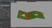
Designing for inspection is key to reliable manufacturing. This article covers practical PCB layout tips to optimize your board for AOI and X-ray inspection helping you reduce defects, false positives, and production delays.

Read More
Embedded thumbnail for How Close Can You Bring a Reference Plane?
How-To's • Jul 8, 2025
How Close Can You Bring a Reference Plane?

Explore our in-depth investigation into practical simulations using both Altium Designer and Polar Si9000. We demonstrate impedance sensitivity analysis and reveal the real limitations of optimizing reference plane proximity for improved signal shielding.

Start Watching
Blog • Jul 7, 2025
Understanding Systems Engineering

Read our brand-new article where we explore the key areas of an engineering project and the different stages of electronic product development from a project execution perspective. From initiation and planning to design, development, validation, testing, and certification, we walk you through each phase to help you understand how successful electronic products are brought to life.

Read More
Embedded thumbnail for Do PCB Thermal Vias Actually Work?
How-To's • Jul 3, 2025
Do PCB Thermal Vias Actually Work?

Are thermal vias really helping your PCB’s heat management? Tech Consultant Zach Peterson dives into simulation data, research, and a controversial article to uncover the truth. Learn why via count and spacing matter more than sheer quantity.

Start Watching
Blog • Jul 2, 2025
PCB First-Pass Yield: Small Decisions That Make a Big Difference

This article highlights how seemingly minor layout choices like trace spacing, component footprints, or stack-up details can dramatically impact whether a board passes fabrication and assembly the first time.

Read More
Blog • Jul 1, 2025
Implementing Design for Supply Chain Principles in Electronic Product Development

Designing with supply chain principles in mind helps you avoid delays, reduce costs, and ensure manufacturability. This article outlines practical strategies for component selection, sourcing, and lifecycle management to make your designs more resilient and production-ready.

Read More
Embedded thumbnail for Stripline Routing Deep Dive: How Close Is Too Close?
How-To's • Jun 30, 2025
Stripline Routing Deep Dive: How Close Is Too Close?

In this video, Zach Peterson takes a deep dive into what happens when reference layers are incorrectly set in a PCB stackup and how that affects impedance, signal integrity, and EMC. He also shares valuable insights into stripline routing proximity issues and best practices for assigning reference planes.

Start Watching
Blog • Jun 27, 2025
Beyond the BOM: How Proactive Component Selection Is Transforming Workflows

Learn how proactive component selection helps you avoid supply chain risks, reduce costs, and design more reliably. Our new article outlines key strategies and shows how tools like Altium 365 support smarter part decisions.

Read More
Blog • Jun 26, 2025
Power Integrity Issues?

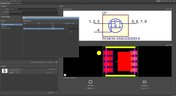
Power problems can be hard to spot until it’s too late. See how easy it is to analyze your power nets, check voltage drops, and improve reliability with Power Analyzer by Keysight - all without leaving your design environment.

Read More
Embedded thumbnail for Coming Soon: Solder Mask Zero Expansion
New in Altium Designer 25 • Jun 25, 2025
Coming Soon: Solder Mask Zero Expansion

Solder Mask Zero Expansion marks a move toward industry alignment, specifically with IPC-7351B and IPC-2581B standards. It changes the default solder mask expansion value from 4 mil to 0 mil. Discover more upcoming updates on our Coming Soon Page.

Start Watching
Blog • Jun 24, 2025
How to Design High-Speed PCBs Without Signal Surprises

Signal issues can sneak in early and cost you later. Read our whitepaper to see how Signal Analyzer by Keysight (inside Altium Designer) helps you catch problems fast and design with confidence.

Read More
Embedded thumbnail for Analog Supply without a Ferrite: Proper Isolation Techniques Explained
How-To's • Jun 20, 2025
Analog Supply without a Ferrite: Proper Isolation Techniques Explained

In our new tutorial, you'll learn why ferrite beads may not be the best choice for isolating analog and digital supply pins on integrated circuits. Zach Peterson debunks common misconceptions about ferrite bead isolation and introduces better alternatives, including dedicated LDOs, precision voltage references, and effective filtering techniques to help you achieve cleaner analog signals in your designs.

Start Watching
Blog • Jun 18, 2025
Beyond Basic Part Selection: Using Supply Chain Data to Validate Choices

Learn how to enhance part selection by using real-time supply chain data. This article shows how integrating insights like availability and lifecycle status helps you make smarter, risk-aware design choices.

Read More
Blog • Jun 17, 2025
Signal Mistakes Are Expensive

See how the Signal Analyzer by Keysight in Altium Designer lets you run signal integrity checks directly within your design environment. Read our article to learn how to effectively manage impedance, return paths, stackups, and more.

Read More
Embedded thumbnail for Enhanced Constraint Manager in Altium Designer 25. Part II: Physical Constraints and Routing Differential Pairs
Enhanced Constraint Manager in Altium Designer 25 • Jun 16, 2025
Enhanced Constraint Manager in Altium Designer 25. Part II: Physical Constraints and Routing Differential Pairs

In the second video of Samer Aldhaher’s "Enhanced Constraint Manager" series, we continue designing a 1 kW, 400 V brushless DC motor driver. This episode focuses on setting physical constraints using constraint sets, routing differential pairs, and demonstrating the Auto Shrinking feature in Altium Designer 25.

Start Watching
  • Show More
Tag (field_common_tag)
Design Reuse Blocks Update
Blog • Sep 14, 2022
Altium Designer 22.9 Update

We are happy to announce that the Altium Designer 22.9 update is now available. Altium Designer 22.9 continues to focus on improving the user experience, as well as performance and stability of the software, based on feedback from our users. Check out the key new features in the What's New section on the left side of this window!

Read More
Dual Rail Voltage Supply
Blog • Sep 13, 2022
Dual Rail Voltage Supply

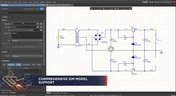
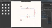
The highest performing operational amplifiers often need a split supply with positive and negative voltages connected to the op amps supply rails. In this project, we’re going to be building a positive/negative dual rail power supply for a differential oscilloscope probe I’m designing. I’m making the power supply a separate project, as a dual rail supply is quite useful to have, and I’m sure I’ll find multiple uses for it in the future.

Read More
Library Importer Interface
Blog • Sep 7, 2022
Library Importer Improvements (former Library Migrator)

Importing file-based libraries from your local computer or network drive to your Altium 365 workspace can be done using the Library Importer. Altium’s Library Migrator was renamed Library Importer—the feature’s name was changed to conform more closely to the tool’s purpose. Not only is its name new, but our team has also made several user experience improvements. We have updated the documentation to reflect this change.

Read More
Blog • Sep 6, 2022
How to Select Copper Foil for High-Frequency PCB Design

The PCB materials industry has spent significant amounts of time developing materials that provide lowest possible signal loss for products with RF applications. For high speed and high frequency designs, losses will limit signal propagation distance and distort signals, and it will create an impedance deviation that can be seen in TDR measurements. In this article, we'll look at the balance between copper foil losses and other types of losses in a PCB, as well as some strategies that are commonly used to overcome roughness.

Read More
Blog • Sep 2, 2022
Altium Designer 22.8 Update

We are happy to announce that the Altium Designer 22.8 update is now available. Altium Designer 22.8 continues to focus on improving the user experience, as well as performance and stability of the software, based on feedback from our users. Check out the key new features in the What's New section on the left side of this window!

Read More
What is Hybrid Beamforming?
Blog • Sep 1, 2022
What is Hybrid Beamforming?

In this article, we’ll look at beamforming implementation in an advanced method combining analog and digital techniques, known as hybrid beamforming. This method blends both digital and analog techniques to create multiple beams and thus reach multiple users with varying intensities. In the case of an RF imaging system or a radar system, hybrid beamforming in a MIMO technique also allows tracking of multiple targets with adjustable resolution.

Read More
Is your via impedance calculator accurate?
Blog • Aug 30, 2022
Why Most Via Impedance Calculators Are Inaccurate

The problem with every via impedance calculator that I have seen is simple: they are incomplete or totally wrong. The “incomplete” part refers to a lack of context; these calculators can roughly reproduce a well-known estimate from a legend like Howard Johnson in his Digital Design textbooks. However, these calculators never provide insight into what they are actually calculating, or where the calculated via impedance is accurate. Keep reading to see why these calculators get it so wrong, as well as the context surrounding via impedance.

Read More
Blog • Aug 25, 2022
Buck Converter Simulation in Altium Designer

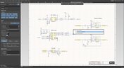
When designing high power circuits (usually very high voltage and/or current), you’ll need to create a regulator from scratch and place it in your PCB layout. It's also the case that you may want to model a real component using discretes in a simulation in order to qualify the system's expected operating regime. As part of buck converter design, you can easily run a buck converter simulation directly in Altium Designer’s schematic editor. Here’s how you can access these features in the newest version of Altium Designer. 

Read More
PCIe 6.0 Overview
Blog • Aug 23, 2022
Overview of the PCIe 6.0 Standard

Just as you get used to PCIe 5.0, they decide to release another standard! The newest iteration of PCIe is Gen6, or PCIe 6.0. PCIe 6.0 brings a doubling of channel bandwidth through introduction of PAM-4 as the signaling method in high-speed differential channels. This signaling method is a first for PCIe, and it’s an important enabler of the doubled data rate we see in the current standard. In this article, I’ll run over the important points in the standard and what PCB designers can expect when designing these channels.

Read More
SPI vs. I2C For Memory Access
Blog • Aug 18, 2022
SPI vs. I2C: How to Choose the Best Protocol for Your Memory Chips

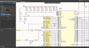
One of the common implementations of SPI and I2C in a PCB layout is as a protocol for reading and writing to an external Flash memory. Flash chips are a very common component in embedded systems and can offer high capacities of non-volatile memory up to Gb values. When choosing a memory chip, you'll want to match the application requirements and functionality with the bus speed you need for read and write operations in your memory chip. There is also the matter of the type of Flash memory you'll need to access (NOR vs. NAND).

Read More
Blog • Aug 16, 2022
Is There an SPI Trace Impedance Requirement?

There is no SPI trace impedance requirement? The reality is that SPI lines only start to need impedance control when the length of the interconnect becomes very long. And because there is no specific impedance requirement in the bus, you have some freedom in channel design and termination. So what exactly qualifies as “very long” and when is some termination method needed? We’ll break it down in this article.

Read More
The Skin Effect and EM Fields
Blog • Aug 11, 2022
The Skin Effect, Current Density, and the Electromagnetic Field

During this year's AltiumLive CONNECT event, I recall receiving an interesting question about the skin effect and the distribution of current due to the presence of ground in coplanar transmission lines. In this article, we'll look at the electric field around a transmission line carrying a signal, and how this might be impacted by the skin effect.

Read More
Packaging for your PCBAs
Blog • Aug 9, 2022
What You Need for PCB Packaging and Shipping

When you get your PCBA back from an assembler, you’ll notice the packaging materials used to pack and ship the PCBA. Those materials are specific to electronics, and if you build products on behalf of clients, it’s important to know the packaging materials used for packing and shipping electronics. In this article I’ll show the main set of materials and equipment used to package electronics assemblies.

Read More
PCB Output files
Blog • Aug 4, 2022
How to Make PCB Gerber Files in Altium Designer Step-by-Step

Once you've got your PCB layout finished and you're ready to start preparing for manufacturing, one of the critical steps is to create PCB Gerber files. When you're ready to create your Gerber files, you need the right set of CAM processor tools that can take data from your PCB layout. In this article, we'll guide you through this process of how to make PCB Gerber files and show some example tasks you might need to perform to generate them.

Read More
Teardrops on Differential Pairs?
Blog • Aug 2, 2022
Should You Place Teardrops on Differential Pairs?

One of the major factors impacting reliability of a PCBA is the use of teardrops on traces in the PCB. Like many aspects of reliability, the considerations also span into the signal integrity domain, particularly as more high-reliability products require greater data handling capabilities and run at higher speeds. In this article, I’ll break down the issues present in teardrop usage on differential pairs and how these may affect impedance.

Read More
Broken PCB
Blog • Jul 28, 2022
The High-Reliability PCBA Design and Test Challenge

High-reliability electronics must go through multiple rounds of testing and qualification to ensure they can withstand their intended operating environment. Designing to performance standards, whether the baseline IPC standards or more stringent industry standards, is the first step in ensuring a reliable circuit board. In this e-book, readers will gain a thorough look into PCB testing and analysis, starting from basic tests performed on bare boards and completed assemblies.

Read More
  • Show More
Tag (field_common_tag)
Embedded thumbnail for Using Polygons on Power Planes
New in Altium Designer 21 • Dec 28, 2020
Using Polygons on Power Planes

Traditionally, a PCB power plane is designed as a negative, that is, the objects placed on a power plane layer become voids in the copper when the board is fabricated. This approach is used because it is more efficient to generate the output data this way, as the bulk of a plane layer is normally copper; voids in the copper are only needed in specific locations such as around non-connected pads, or as separation voids when the plane is divided into different voltage regions.

Start Watching
Embedded thumbnail for Enhanced Polar Grid Support
New in Altium Designer 21 • Dec 28, 2020
Enhanced Polar Grid Support

Component placement is one of the main steps in board design. And in specific boards of a circular shape, it is convenient to use a polar grid for the location of components. Altium Designer 21 brings several improvements to the polar grid. Now, when a component is positioned in a polar grid, its properties additionally display location coordinates relative to this grid. Using them, you can quickly arrange the components in the right places. And moving the component off the grid, polar coordinates are automatically disabled.

Start Watching
Embedded thumbnail for New PCB Length Tuning Patterns
New in Altium Designer 21 • Dec 28, 2020
New PCB Length Tuning Patterns

Length matching is a critical element of high-speed design, usually solved by carefully tuning the lengths of critical routes. This release sees extensive improvements to both single-sided and differential pair length tuning capabilities. Length tuning now supports all three popular tuning patterns: Trombone, Sawtooth, and Accordion. If you are working with lower speed or lower frequency signals, you can get away with trombone tuning. For the Trombone patterns, the polygonal area that the pattern is constructed within can be thought of as a sleeve.

Start Watching
Embedded thumbnail for Expressions Library for Frequently Used Rules
New in Altium Designer 21 • Dec 28, 2020
Expressions Library for Frequently Used Rules

When working with design rules, we often use different scopes of the rules. To simplify the repetitive process of creating advanced type rules, the new Altium Designer 21 Rule Editor has the ability to save query-based object mapping scopes in a scoped library. To do this, it is enough to export the request by clicking on it with RMB. The library is presented through the Properties panel, where custom scopes can be edited, new ones added, and later reused in other custom constraint rules.

Start Watching
Embedded thumbnail for Constraint Rule Violations
New in Altium Designer 21 • Dec 28, 2020
Constraint Rule Violations

Enabled design constraint rules are applied to the current board design through a range of mechanisms, such as live Online Design Rule Checking, the batch Design Rule Checker or selectively run from the PCB Rules and Violations panel. Violations of those constraint Rules – where the specified and scoped limits are exceeded – are indicated through board graphics, panel entries and reports. With the introduction of a new Rules Editor in Altium Designer 21, violations of these rules are now displayed in the Rules Editor itself.

Start Watching
Embedded thumbnail for Table-based Approach for Design Rules and Constraints
New in Altium Designer 21 • Dec 28, 2020
Table-based Approach for Design Rules and Constraints

Define and assign a specific list of rules and constraints to all critical design elements, such as components, nets, and LVDS.

Start Watching
Embedded thumbnail for Comprehensive Simulation Model Support
New in Altium Designer 21 • Dec 28, 2020
Comprehensive Simulation Model Support

Having accurate SPICE models is critical to the success of your simulation. Altium Designer now supports analog PSpice, LTspice, and more including generic component SPICE models for when you can’t find company models. Generic components contain Spice model parameters to simplify simulation. When you are done with simulation, quickly replace your generic components with an existing component to finish your design.

Start Watching
Embedded thumbnail for Easy to Start Simulations
New in Altium Designer 21 • Dec 28, 2020
Easy to Start Simulations

0:00 Simulation Dashboard Panel Following on from the recent introduction of an advanced new SPICE Simulation engine for Altium Designer, the latest round of Simulation updates focuses on user interface. A major component of the Altium Designer Simulation user interface updates is the introduction of the Simulation Dashboard panel. The panel offers a greatly simplified approach to checking, configuring, running and reviewing simulations.

Start Watching
Embedded thumbnail for Rigid-Flex Board Planning Mode
New in Altium Designer 21 • Dec 28, 2020
Rigid-Flex Board Planning Mode

This new release of Altium Designer 21 includes significant improvements to the Rigid-Flex board designs. Along with many bug fixes and enhancements, the next phase of Altium Rigid-Flex technology development is providing functional improvements. It is now possible to create new board regions by primitives using the appropriate command from the Design » Board Shape menu. The properties of all created regions are now displayed in the Properties panel where you can edit the name of each region and define the previously created stacks for each region of the board.

Start Watching
Embedded thumbnail for Component Pin to Multiple Pad Mapping
New in Altium Designer 21 • Dec 28, 2020
Component Pin to Multiple Pad Mapping

This release introduces flexible pin to pad mapping capabilities for managed components. Enhancements to the Single Component Editor and the introduction of a new Pins panel allow component symbol pins to be mapped to any component footprint pad, or any number of footprint pads. The Pins panel, opened from the editor's button, allows the default one-to-one pin-pad mapping to be changed to a custom relationship, such as one pin being connected to multiple footprint pads – or any other non-aligned pin to pad number relationship.

Start Watching
Embedded thumbnail for Enhanced Navigation by Nets in Schematic - Altium Designer 21 What's New
New in Altium Designer 21 • Dec 28, 2020
Enhanced Navigation by Nets in Schematic - Altium Designer 21 What's New

Altium Designer 21 brings many improvements to the schematic editor aimed at visualizing circuits and improving navigation through them in multi-sheet and hierarchical designs. By holding Alt and clicking on the net, All schematic instances of the net are highlighted, while other objects are dimmed, to visibly indicate the signal/power propagation in the design using one simple action. The changes also affected the Identification of net names. Now logical and physical names of a net are displayed in the properties panel as well as when you hover over this wire.

Start Watching
Embedded thumbnail for Intelligent Schematic Insights
New in Altium Designer 21 • Dec 28, 2020
Intelligent Schematic Insights

Due to advances in the format and compilation of the Altium Designer data model, schematic Wire objects have now evolved from a simple graphical object to a more advanced form that can be directly associated with electrical parameters. As a result, the Wire mode of the Properties panel has been updated to provide an expanded set of options and a wider range of information. The new additions include a General section for net parameter options and information, and a Parameters section that lists the User Parameters, Rules and Net Classes associated with the Wire's assigned net.

Start Watching
Embedded thumbnail for Start Your Schematic with Generic Components
New in Altium Designer 21 • Dec 28, 2020
Start Your Schematic with Generic Components

It can be challenging to pick the right components when working on a new schematic. You have to consider availability, cost, and various parametric requirements. What if you could place a component to complete your design and quickly replace it when you are ready for layout? Introducing new Generic Components. Simply provide generic parameters, such as Value or Footprint, to greatly speed-up your capturing process while eliminating the need to search for specific Part Numbers or creating a needed component from scratch.

Start Watching
Embedded thumbnail for MCAD CoDesigner Overview
Working with MCAD CoDesigner extension • Dec 21, 2020
MCAD CoDesigner Overview

The MCAD CoDesigner in Altium Designer allows for seamless design transfer between the Electrical and Mechanical designers. In this overview, we’ll show you how to transfer from Altium Designer to your CAD tool of choice, then how to resize the board, add mounting holes, add a new connector, and update the board design in Altium Designer.

Start Watching
Embedded thumbnail for Bringing an MCAD Enclosure to ECAD
Working with MCAD CoDesigner extension • Nov 16, 2020
Bringing an MCAD Enclosure to ECAD

The Altium Designer MCAD CoDesigner panel and extension make it easy to move a 3D enclosure model from your MCAD tool to Altium Designer. We'll show you how and what to watch out for while your transferring your enclosure model to Altium Designer.

Start Watching
Embedded thumbnail for How to Perform a Component Search in Concord Pro - Altium Academy
How-To's • Oct 28, 2020
How to Perform a Component Search in Concord Pro - Altium Academy

In this video, I'll show you how to perform a component search in the Components Panel. Learn how to perform a component search in the Components Panel while using Altium Concord Pro to effectively host all your component libraries from Altium Designer. You can always locate any particular component using this library navigation and place it on your schematic with pricing information from global suppliers. This availability and pricing information gets updated daily directly from the suppliers so you will always get fresh, up to date information. 

Start Watching
  • Show More
Tag (field_common_tag)
Altium Enterprise
On-Demand Webinar • May 10, 2025
Streamline your customer relation with Altium 365 Enterprise
Join our webinar designed for engineers and users in EMS companies
Watch Now
PCB
On-Demand Webinar • May 1, 2025
Altium Designer Overview
Altium Designer is the #1 PCB design tool for a reason. Join us for this live webinar and get an inside look at Altium’s world-class PCB design solution. See for yourself why design teams around the globe are making the switch to Altium Designer. Register now!
Watch Now
Enterprise
On-Demand Webinar • Apr 25, 2025
Altium Customization with Scripting or Low-Code
See how scripting, low-code, no-code, and API integrations can help you work more efficiently—without extra setup or complex systems.
Watch Now
A365 Webinar: Altium BOM Portal - From PCB Design to Parts Ordering in Minutes
On-Demand Webinar • Apr 21, 2025
Altium 365 BOM Portal - From PCB Design to Parts Ordering in Minutes
Join us to learn how to reduce sourcing time by up to 70% using Altium 365 BOM Portal.
Watch Now
April 2025 COM Webinar
On-Demand Webinar • Apr 17, 2025
Advanced xSignal and Impedance Control Techniques
We are hosting a free webinar on advanced xSignal configuration and impedance control techniques in Altium Designer to help you tackle signal integrity challenges. Register now to enhance your design skills.
Watch Now
Altium Enterprise
On-Demand Webinar • Mar 25, 2025
Unlocking the full potential of your design team with Altium's enterprise solution
See how Altium's enterprise solution can help you meet your electronic product design goals
Watch Now
Transmission line
On-Demand Webinar • Mar 4, 2025
Optimizing Layer Stackup and Impedance for High-Speed PCB Design
Learn how to master the layer stack manager to efficiently create stackups, manage materials, and ensure optimal design performance.
Watch Now
Harness design
On-Demand Webinar • Mar 2, 2025
Design Smarter - Harness, Multi-board, and MCAD CoDesign in Action
Discover how the latest Harness, Multi-board, and MCAD CoDesign tools can revolutionize your PCB design workflow.
Watch Now
ADv25
On-Demand Webinar • Jan 30, 2025
6 Reasons to Switch Design Tools
Come see how Altium Designer, the industry standard for PCB design, combined with Altium 365 delivers the world’s first connected PCB design experience.
Watch Now
PCB CoDesign
On-Demand Webinar • Jan 29, 2025
Level Up Your Team's Productivity with Altium
Discover how to create an efficient, collaborative, and transparent design process for your team!
Watch Now
Assembly variants
On-Demand Webinar • Jan 9, 2025
Designing with Assembly Variants
Join us to learn best practices and get into the details about setting up variants in your designs and speeding up your project development.
Watch Now
Single layer PCB
On-Demand Webinar • Jan 8, 2025
Optimized for Success - Advanced PCB Features in Altium Designer
This webinar will show you how to use the latest PCB Layout, signal integrity analysis, and component management design tools in Altium Designer.
Watch Now
Rigid flex
On-Demand Webinar • Dec 19, 2024
How To Use Modern Rigid-Flex Substrates
Join us in this webinar where we’ll go over how you can easily create your own flex design.
Watch Now
Power Analyzer
On-Demand Webinar • Oct 29, 2024
Power Integrity Made Simple
Power Analyzer by Keysight in Altium Designer makes it easy to resolve PDN issues that arise during the board design process within a unified design environment.
Watch Now
Electronic Component Traceability
On-Demand Webinar • Oct 25, 2024
Ensuring Electronic Component Traceability From Idea to Innovation
Watch the webinar to learn how to achieve full transparency, improve collaboration, and ensure compliance throughout your entire supply chain—whether you are sourcing domestically or abroad.
Watch Now
Why Altium Designer is Your Next Step for PCB Design
On-Demand Webinar • Oct 24, 2024
Why Altium Designer is Your Next Step for PCB Design
Join us to see how moving to Altium Designer can enable resilient and scalable designs while streamlining your entire workflow.
Watch Now
  • Show More
Tag (field_common_tag)
Loading
Loading...
Share link
Share with
Search by Update
Version
Update
25 26 24 23 22
25.0 25.1 25.2 25.3 25.4 25.5 25.6 25.7 25.8 25.9
26.1 26.2
24.10 24.9 24.8 24.7 24.6 24.5 24.4 24.3 24.2 24.1 24.0
23.11 23.10 23.9 23.8 23.7 23.6 23.5 23.4 23.3 23.2 23.1 23.0
22.11 22.10 22.9 22.8 22.7 22.6 22.5 22.4 22.3