
Main navigation

  • Home
  • Discover
  • Learning Center
  • What’s New

Second main navigation

  • Altium Community
  • Support
  • Documentation
×

Results

  • Updates
  • Blog 570
  • Video 539
  • Webinar 86
  • Playlist 53
Filters:
Tag (field_common_tag)
Embedded thumbnail for How Close Can You Bring a Reference Plane?
How-To's • Jul 8, 2025
How Close Can You Bring a Reference Plane?

Explore our in-depth investigation into practical simulations using both Altium Designer and Polar Si9000. We demonstrate impedance sensitivity analysis and reveal the real limitations of optimizing reference plane proximity for improved signal shielding.

Start Watching
Blog • Jul 7, 2025
Understanding Systems Engineering

Read our brand-new article where we explore the key areas of an engineering project and the different stages of electronic product development from a project execution perspective. From initiation and planning to design, development, validation, testing, and certification, we walk you through each phase to help you understand how successful electronic products are brought to life.

Read More
Embedded thumbnail for Do PCB Thermal Vias Actually Work?
How-To's • Jul 3, 2025
Do PCB Thermal Vias Actually Work?

Are thermal vias really helping your PCB’s heat management? Tech Consultant Zach Peterson dives into simulation data, research, and a controversial article to uncover the truth. Learn why via count and spacing matter more than sheer quantity.

Start Watching
Blog • Jul 2, 2025
PCB First-Pass Yield: Small Decisions That Make a Big Difference

This article highlights how seemingly minor layout choices like trace spacing, component footprints, or stack-up details can dramatically impact whether a board passes fabrication and assembly the first time.

Read More
Blog • Jul 1, 2025
Implementing Design for Supply Chain Principles in Electronic Product Development

Designing with supply chain principles in mind helps you avoid delays, reduce costs, and ensure manufacturability. This article outlines practical strategies for component selection, sourcing, and lifecycle management to make your designs more resilient and production-ready.

Read More
Embedded thumbnail for Stripline Routing Deep Dive: How Close Is Too Close?
How-To's • Jun 30, 2025
Stripline Routing Deep Dive: How Close Is Too Close?

In this video, Zach Peterson takes a deep dive into what happens when reference layers are incorrectly set in a PCB stackup and how that affects impedance, signal integrity, and EMC. He also shares valuable insights into stripline routing proximity issues and best practices for assigning reference planes.

Start Watching
Blog • Jun 27, 2025
Beyond the BOM: How Proactive Component Selection Is Transforming Workflows

Learn how proactive component selection helps you avoid supply chain risks, reduce costs, and design more reliably. Our new article outlines key strategies and shows how tools like Altium 365 support smarter part decisions.

Read More
Blog • Jun 26, 2025
Power Integrity Issues?

Power problems can be hard to spot until it’s too late. See how easy it is to analyze your power nets, check voltage drops, and improve reliability with Power Analyzer by Keysight - all without leaving your design environment.

Read More
Embedded thumbnail for Coming Soon: Solder Mask Zero Expansion
New in Altium Designer 25 • Jun 25, 2025
Coming Soon: Solder Mask Zero Expansion

Solder Mask Zero Expansion marks a move toward industry alignment, specifically with IPC-7351B and IPC-2581B standards. It changes the default solder mask expansion value from 4 mil to 0 mil. Discover more upcoming updates on our Coming Soon Page.

Start Watching
Blog • Jun 24, 2025
How to Design High-Speed PCBs Without Signal Surprises

Signal issues can sneak in early and cost you later. Read our whitepaper to see how Signal Analyzer by Keysight (inside Altium Designer) helps you catch problems fast and design with confidence.

Read More
Embedded thumbnail for Analog Supply without a Ferrite: Proper Isolation Techniques Explained
How-To's • Jun 20, 2025
Analog Supply without a Ferrite: Proper Isolation Techniques Explained

In our new tutorial, you'll learn why ferrite beads may not be the best choice for isolating analog and digital supply pins on integrated circuits. Zach Peterson debunks common misconceptions about ferrite bead isolation and introduces better alternatives, including dedicated LDOs, precision voltage references, and effective filtering techniques to help you achieve cleaner analog signals in your designs.

Start Watching
Blog • Jun 18, 2025
Beyond Basic Part Selection: Using Supply Chain Data to Validate Choices

Learn how to enhance part selection by using real-time supply chain data. This article shows how integrating insights like availability and lifecycle status helps you make smarter, risk-aware design choices.

Read More
Blog • Jun 17, 2025
Signal Mistakes Are Expensive

See how the Signal Analyzer by Keysight in Altium Designer lets you run signal integrity checks directly within your design environment. Read our article to learn how to effectively manage impedance, return paths, stackups, and more.

Read More
Embedded thumbnail for Enhanced Constraint Manager in Altium Designer 25. Part II: Physical Constraints and Routing Differential Pairs
Enhanced Constraint Manager in Altium Designer 25 • Jun 16, 2025
Enhanced Constraint Manager in Altium Designer 25. Part II: Physical Constraints and Routing Differential Pairs

In the second video of Samer Aldhaher’s "Enhanced Constraint Manager" series, we continue designing a 1 kW, 400 V brushless DC motor driver. This episode focuses on setting physical constraints using constraint sets, routing differential pairs, and demonstrating the Auto Shrinking feature in Altium Designer 25.

Start Watching
Embedded thumbnail for Auto-tuning Your Way to Faster PCB Design
Altium Designer's 25 Quantitative Benefits • Jun 13, 2025
Auto-tuning Your Way to Faster PCB Design

Watch how the Auto Tuning feature in Altium Designer 25 delivers optimized DDR4 routing in a single click! Fewer steps, massive time savings. Try our Benefit Calculator to estimate your own time and cost savings.

Start Watching
Blog • Jun 12, 2025
Twice the Insight. One Seamless Simulation Bundle

Ensure power and signal integrity with the Keysight Bundle in Altium Designer. Catch issues early, reduce rework, and optimize your PCBs - all within one integrated environment featuring Signal & Power Analyzer.

Read More
  • Show More
Tag (field_common_tag)
Blog • Jul 10, 2023
Analog Solar Tracker Project

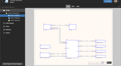
In this article you can learn about light sensors while building an analog solar panel tracking system. This open-source project covers multi-channel design, window comparators, driving motors, and photosensors.

Read More
Blog • Jul 6, 2023
Concept Phase – Initial CAD Design

We are continuing our journey through the open-source laptop project. This article explains an initialization of CAD design process from the early concept and brainstorming phase.

Read More
Blog • Jul 5, 2023
Expert Tips for Safely Powering Up Your New PCB for the First Time

In this blog we will show you the strategies to minimize the risk of damage to circuit boards during the initial power-up process.

Read More
Blog • Jun 30, 2023
High-Speed PCB Design Tips

Essential tips for high-speed PCB designs, and when you need to start being concerned about how and where you route your traces.

Read More
mb
Blog • Jun 28, 2023
Altium 365 Web Viewer's Multi-board Schematic (MBS) and Assembly (MBA)
We are pleased to introduce the Altium 365 Multi-board Design View, which supports viewing Multi-board Schematic (MBS) and Assembly (MBA) documents directly within the browser.
Read More
Blog • Jun 27, 2023
MIDs Make a Comeback as Vertical SMD Modules for Your PCB

If you've ever wanted to mount components vertically, but without the expense of a flex section this article is for you. You can use an MID in your PCB.

Read More
Blog • Jun 26, 2023
Everything You Need to Know about Conformal Coating

Explore the basics of conformal coating with us. Conformal coating is a protective layer applied to electronic circuits to guard against environmental factors such as moisture and dust.

Read More
Introduction to Open Source Laptop Project
Blog • Jun 15, 2023
Introduction to Open Source Laptop Project

We have started a very exciting journey into the creation of an open source laptop project. This project will be an ongoing one, with our community able interactively participate. By utilizing Altium 365 users will be able to view, comment on, and download design files. This will be a great learning experience for new and experienced PCB designers.

Read More
g
Blog • Jun 9, 2023
Guest Users in Altium 365

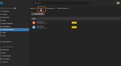
Altium 365 has introduced a new feature that enhances visibility and improves project management for external users. This feature introduces the concept of "Guests" to identify and differentiate external users from workspace members.

Read More
SOC 2 Type 2
Blog • Jun 7, 2023
Altium 365 SOC 2 Type 2

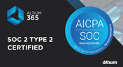
We are pleased to announce that Altium 365 has achieved SOC 2 Type 2 certification, demonstrating our dedication to upholding the highest standards of security, availability, processing integrity, confidentiality, and privacy.

Read More
invite
Blog • Jun 5, 2023
Workspace Invitation by Non-Admins in Altium 365

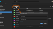
We are thrilled to announce a new feature in Altium 365 that empowers non-admin users to create invitation requests for new users to join the workspace. Previously, only workspace administrators could invite new users, limiting the flexibility to bring in additional workspace members.

Read More
Blog • Jun 1, 2023
Unlock the power of efficiency with Altium 365!

According to a commissioned Study conducted by Forrester Consulting on behalf of Altium, our cloud-based electronics design platform saves 159 hours per engineer annually, streamlines the production cycle, and reduces alternative component sourcing by 65%.

For a comprehensive look at the benefits, download the full Forrester Study and infographic today and don't miss to watch our webinar featuring Fabian Winkler, Product Marketing Manager at Altium 365, and guest speaker Casey Sirotnak, Sr Consultant TEI Project Lead at Forrester.

Read More
SuperSpreader
Blog • May 26, 2023
Introducing Altium 365 Contractor Portal

We are thrilled to introduce the Altium 365 Contractor Portal, an exciting new platform designed to connect you with trusted partners who are experts in electronic design and Altium 365. This portal offers you a secure and efficient space to connect with professionals specializing in Altium 365.

Read More
plm
Blog • May 5, 2023
PLM Configurator in Altium 365

The new PLM Integration Configurator is a useful tool for product development teams using Altium 365. This tool allows users to configure and customize their PLM integration to best fit their team's needs.

Read More
MCAD
Blog • May 1, 2023
MCAD-ECAD Collaboration Workflow

Join our webinar to discover the most efficient MCAD-ECAD collaboration workflow. Discover the efficient MCAD-ECAD collaboration workflow with Altium MCAD CoDesigner during our upcoming webinar. Join us to see how this software streamlines collaboration and enables secure sharing of the final release package.

Read More
Dictionary
Blog • Apr 27, 2023
Dictionaries (Allowed Values for Component Properties)

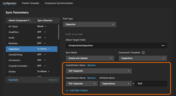
The Dictionaries feature in Altium 365 is a real game-changer for maintaining the quality of your component library and minimizing errors and duplicates in parameter values. This feature promotes consistency and accuracy throughout the design process by establishing a set of allowed values for parameters.

Read More
  • Show More
Tag (field_common_tag)
Embedded thumbnail for Drawing Tools for Pro Schematics in Altium
How-To's • Oct 16, 2025
Drawing Tools for Pro Schematics in Altium

In our brand-new tutorial, you’ll learn how to create professional-looking schematics in Altium using built-in drawing tools and features. We’ll show you how to add custom title blocks, revision histories, tables of contents, block diagrams, and color schemes to make your schematics stand out.

Start Watching
Embedded thumbnail for 3 GHz RF Amplifier Deep Dive
How-To's • Oct 14, 2025
3 GHz RF Amplifier Deep Dive

Check out our design review of a 3.6 GHz RF amplifier! This in-depth analysis highlights schematic issues, PCB layout challenges, and key RF design principles to help you build better high-frequency circuits.

Start Watching
Embedded thumbnail for The Right Way to Use SIG/GND/PWR/SIG Stackups
How-To's • Oct 8, 2025
The Right Way to Use SIG/GND/PWR/SIG Stackups

Find out how to properly implement signal-ground-power-signal stackups in 4-layer PCB designs. Check out our tutorial from Zach Peterson, where he explains when to use dedicated power layers, how to route signals correctly over split power planes, and common mistakes to avoid for optimal EMI performance and signal integrity.

Start Watching
Embedded thumbnail for Altium Training - Design Environment: Documents and Panels
Altium Training • Oct 6, 2025
Altium Training - Design Environment: Documents and Panels

In our new tutorial, we explore different panel display modes, including docked, floating, and tabbed grouping arrangements. Effective panel management is essential for creating an efficient design environment tailored to your specific workflow requirements.

Start Watching
Embedded thumbnail for Mechanically Drilled Blind & Buried Vias: PCB Design Rules Explained
How-To's • Oct 1, 2025
Mechanically Drilled Blind & Buried Vias: PCB Design Rules Explained

Discover the essential design rules and manufacturing processes for mechanically drilled blind and buried vias in PCB layouts in this comprehensive tutorial. We cover the stack drill-and-plate fabrication process, aspect ratio limitations, sub-lamination design, and copper weight considerations. You’ll also learn how these vias differ from HDI microvias and gain a clear understanding of the critical design constraints needed for successful PCB manufacturing.

Start Watching
Embedded thumbnail for Altium Training - Design Environment: Navigation with Schematic Workspace
Altium Training • Sep 29, 2025
Altium Training - Design Environment: Navigation with Schematic Workspace

Discover the most important navigation techniques for the schematic workspace using both mouse and keyboard controls. In this tutorial video, you’ll learn how to use the View menu commands for document fitting, area zooming, and object selection, along with advanced navigation shortcuts. Master mouse-based panning and zooming, explore Ctrl key combinations, and practice arrow key movements - all designed to simplify your workflow in the PCB design process.

Start Watching
Embedded thumbnail for Altium Training - Design Environment: The Altium Environment
How-To's • Sep 23, 2025
Altium Training - Design Environment: The Altium Environment

Get familiar with the core workspace layout and navigation methods. In this video, you’ll see how to open schematic and PCB documents, work within the unified design environment, and move between multiple open files using document tabs and keyboard shortcuts.

Start Watching
Embedded thumbnail for Altium Training - Design Environment: Opening a Project from a Local Drive
Altium Training • Sep 18, 2025
Altium Training - Design Environment: Opening a Project from a Local Drive

Get your PCB design workflow off to a smooth start. This Altium tutorial walks you through opening projects from your local directory - a core skill that keeps your process efficient and organized from day one.

Start Watching
Embedded thumbnail for Altium Essentials: Design Environment
Altium Training • Sep 16, 2025
Altium Essentials: Design Environment

Take control of your PCB design workflow with Altium Essentials: Design Environment. This tutorial module guides you through the fundamentals of workspace management, from handling panels and documents to mastering menus, context commands, and time-saving shortcuts.

Start Watching
Embedded thumbnail for What Makes a Great PCB Design Review Submission?
How-To's • Sep 11, 2025
What Makes a Great PCB Design Review Submission?

Turn your PCB designs into professional-grade submissions. At Altium, we reveal the key practices that transform schematics, layouts, and documentation into review-ready work that stands out. Watch our brand-new tutorial and take your PCB design process to the next level.

Start Watching
Embedded thumbnail for Altium Training - Workspace Folder Structure: Opening the Explorer Panel
Altium Training • Sep 9, 2025
Altium Training - Workspace Folder Structure: Opening the Explorer Panel

Discover the key ways to access the Explorer panel in Altium Designer with this step-by-step tutorial. The video walks you through four different methods, giving you the freedom to choose the approach that best fits your workflow.

Start Watching
Embedded thumbnail for Altium Essentials: Workspace Folder Structure Overview
Altium Training • Sep 3, 2025
Altium Essentials: Workspace Folder Structure Overview

Altium Essentials: Workspace Folder Structure is a tutorial series designed for PCB designers who are learning the fundamentals of navigating an Altium workspace. This playlist walks through key Explorer panel skills, including multiple ways to open it (via keyboard shortcuts, menus, panel buttons, and workspaces), navigating projects, and understanding the panel’s six core information areas.

Start Watching
Embedded thumbnail for NFC Reader Project Part One: Schematics to PCB in Altium
How-To's • Aug 28, 2025
NFC Reader Project Part One: Schematics to PCB in Altium

Check out our new, in-depth NFC Reader Project tutorial! In this two-part video series, we design an ESP32-based NFC transceiver board from schematics to PCB layout. In Part 1, we dive into the TRF7970A NFC chip from Texas Instruments and guide you step-by-step through the complete design process in Altium.

Start Watching
Embedded thumbnail for HDI PCB Design Review: nRF52840 Via Sizing & Stack-Up Best Practices
How-To's • Aug 25, 2025
HDI PCB Design Review: nRF52840 Via Sizing & Stack-Up Best Practices

Explore key HDI design strategies, from calculating aspect ratios and optimizing pad diameters to managing drill tolerances and refining stack-ups for improved signal integrity. This comprehensive review highlights practical solutions to common HDI challenges, including via-in-pad layouts, clearance violations, and layer thickness adjustments for both mechanical and laser drilling processes.

Start Watching
Embedded thumbnail for 13 Common PCB Problems & How to Fix Them in Altium
How-To's • Aug 20, 2025
13 Common PCB Problems & How to Fix Them in Altium

Stop wasting time on manufacturing rework. This guide shows you how to set up Altium’s design rules to prevent the 13 PCB issues that most often derail production ensuring your boards are built right the first time.

Start Watching
Embedded thumbnail for What's Inside Your MCU Module?
How-To's • Aug 18, 2025
What's Inside Your MCU Module?

Are you curious about what’s inside a microcontroller module? Join us as we take a closer look at the Texas Instruments CC3235 Wi-Fi module under the microscope. In this video, we’ll explore its key components, including the microcontroller, flash memory, and RF circuitry, and explain how they work together to power the module.

Start Watching
  • Show More
Tag (field_common_tag)
Altium Enterprise
On-Demand Webinar • May 10, 2025
Streamline your customer relation with Altium 365 Enterprise
Join our webinar designed for engineers and users in EMS companies
Watch Now
PCB
On-Demand Webinar • May 1, 2025
Altium Designer Overview
Altium Designer is the #1 PCB design tool for a reason. Join us for this live webinar and get an inside look at Altium’s world-class PCB design solution. See for yourself why design teams around the globe are making the switch to Altium Designer. Register now!
Watch Now
Enterprise
On-Demand Webinar • Apr 25, 2025
Altium Customization with Scripting or Low-Code
See how scripting, low-code, no-code, and API integrations can help you work more efficiently—without extra setup or complex systems.
Watch Now
A365 Webinar: Altium BOM Portal - From PCB Design to Parts Ordering in Minutes
On-Demand Webinar • Apr 21, 2025
Altium 365 BOM Portal - From PCB Design to Parts Ordering in Minutes
Join us to learn how to reduce sourcing time by up to 70% using Altium 365 BOM Portal.
Watch Now
April 2025 COM Webinar
On-Demand Webinar • Apr 17, 2025
Advanced xSignal and Impedance Control Techniques
We are hosting a free webinar on advanced xSignal configuration and impedance control techniques in Altium Designer to help you tackle signal integrity challenges. Register now to enhance your design skills.
Watch Now
Altium Enterprise
On-Demand Webinar • Mar 25, 2025
Unlocking the full potential of your design team with Altium's enterprise solution
See how Altium's enterprise solution can help you meet your electronic product design goals
Watch Now
Transmission line
On-Demand Webinar • Mar 4, 2025
Optimizing Layer Stackup and Impedance for High-Speed PCB Design
Learn how to master the layer stack manager to efficiently create stackups, manage materials, and ensure optimal design performance.
Watch Now
Harness design
On-Demand Webinar • Mar 2, 2025
Design Smarter - Harness, Multi-board, and MCAD CoDesign in Action
Discover how the latest Harness, Multi-board, and MCAD CoDesign tools can revolutionize your PCB design workflow.
Watch Now
ADv25
On-Demand Webinar • Jan 30, 2025
6 Reasons to Switch Design Tools
Come see how Altium Designer, the industry standard for PCB design, combined with Altium 365 delivers the world’s first connected PCB design experience.
Watch Now
PCB CoDesign
On-Demand Webinar • Jan 29, 2025
Level Up Your Team's Productivity with Altium
Discover how to create an efficient, collaborative, and transparent design process for your team!
Watch Now
Assembly variants
On-Demand Webinar • Jan 9, 2025
Designing with Assembly Variants
Join us to learn best practices and get into the details about setting up variants in your designs and speeding up your project development.
Watch Now
Single layer PCB
On-Demand Webinar • Jan 8, 2025
Optimized for Success - Advanced PCB Features in Altium Designer
This webinar will show you how to use the latest PCB Layout, signal integrity analysis, and component management design tools in Altium Designer.
Watch Now
Rigid flex
On-Demand Webinar • Dec 19, 2024
How To Use Modern Rigid-Flex Substrates
Join us in this webinar where we’ll go over how you can easily create your own flex design.
Watch Now
Power Analyzer
On-Demand Webinar • Oct 29, 2024
Power Integrity Made Simple
Power Analyzer by Keysight in Altium Designer makes it easy to resolve PDN issues that arise during the board design process within a unified design environment.
Watch Now
Electronic Component Traceability
On-Demand Webinar • Oct 25, 2024
Ensuring Electronic Component Traceability From Idea to Innovation
Watch the webinar to learn how to achieve full transparency, improve collaboration, and ensure compliance throughout your entire supply chain—whether you are sourcing domestically or abroad.
Watch Now
Why Altium Designer is Your Next Step for PCB Design
On-Demand Webinar • Oct 24, 2024
Why Altium Designer is Your Next Step for PCB Design
Join us to see how moving to Altium Designer can enable resilient and scalable designs while streamlining your entire workflow.
Watch Now
  • Show More
Tag (field_common_tag)
Loading
Loading...
Share link
Share with
Search by Update
Version
Update
25 26 24 23 22
25.0 25.1 25.2 25.3 25.4 25.5 25.6 25.7 25.8 25.9
26.1 26.2
24.10 24.9 24.8 24.7 24.6 24.5 24.4 24.3 24.2 24.1 24.0
23.11 23.10 23.9 23.8 23.7 23.6 23.5 23.4 23.3 23.2 23.1 23.0
22.11 22.10 22.9 22.8 22.7 22.6 22.5 22.4 22.3