
Main navigation

  • Home
  • Discover
  • Learning Center
  • What’s New

Second main navigation

  • Altium Community
  • Support
  • Documentation
×

Results

  • Updates
  • Blog 570
  • Video 540
  • Webinar 87
  • Playlist 53
Filters:
Tag (field_common_tag)
Blog • Jul 9, 2025
How to Make Your PCB Layout AOI and X-Ray Friendly

Designing for inspection is key to reliable manufacturing. This article covers practical PCB layout tips to optimize your board for AOI and X-ray inspection helping you reduce defects, false positives, and production delays.

Read More
Embedded thumbnail for How Close Can You Bring a Reference Plane?
How-To's • Jul 8, 2025
How Close Can You Bring a Reference Plane?

Explore our in-depth investigation into practical simulations using both Altium Designer and Polar Si9000. We demonstrate impedance sensitivity analysis and reveal the real limitations of optimizing reference plane proximity for improved signal shielding.

Start Watching
Blog • Jul 7, 2025
Understanding Systems Engineering

Read our brand-new article where we explore the key areas of an engineering project and the different stages of electronic product development from a project execution perspective. From initiation and planning to design, development, validation, testing, and certification, we walk you through each phase to help you understand how successful electronic products are brought to life.

Read More
Embedded thumbnail for Do PCB Thermal Vias Actually Work?
How-To's • Jul 3, 2025
Do PCB Thermal Vias Actually Work?

Are thermal vias really helping your PCB’s heat management? Tech Consultant Zach Peterson dives into simulation data, research, and a controversial article to uncover the truth. Learn why via count and spacing matter more than sheer quantity.

Start Watching
Blog • Jul 2, 2025
PCB First-Pass Yield: Small Decisions That Make a Big Difference

This article highlights how seemingly minor layout choices like trace spacing, component footprints, or stack-up details can dramatically impact whether a board passes fabrication and assembly the first time.

Read More
Blog • Jul 1, 2025
Implementing Design for Supply Chain Principles in Electronic Product Development

Designing with supply chain principles in mind helps you avoid delays, reduce costs, and ensure manufacturability. This article outlines practical strategies for component selection, sourcing, and lifecycle management to make your designs more resilient and production-ready.

Read More
Embedded thumbnail for Stripline Routing Deep Dive: How Close Is Too Close?
How-To's • Jun 30, 2025
Stripline Routing Deep Dive: How Close Is Too Close?

In this video, Zach Peterson takes a deep dive into what happens when reference layers are incorrectly set in a PCB stackup and how that affects impedance, signal integrity, and EMC. He also shares valuable insights into stripline routing proximity issues and best practices for assigning reference planes.

Start Watching
Blog • Jun 27, 2025
Beyond the BOM: How Proactive Component Selection Is Transforming Workflows

Learn how proactive component selection helps you avoid supply chain risks, reduce costs, and design more reliably. Our new article outlines key strategies and shows how tools like Altium 365 support smarter part decisions.

Read More
Blog • Jun 26, 2025
Power Integrity Issues?

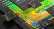
Power problems can be hard to spot until it’s too late. See how easy it is to analyze your power nets, check voltage drops, and improve reliability with Power Analyzer by Keysight - all without leaving your design environment.

Read More
Embedded thumbnail for Coming Soon: Solder Mask Zero Expansion
New in Altium Designer 25 • Jun 25, 2025
Coming Soon: Solder Mask Zero Expansion

Solder Mask Zero Expansion marks a move toward industry alignment, specifically with IPC-7351B and IPC-2581B standards. It changes the default solder mask expansion value from 4 mil to 0 mil. Discover more upcoming updates on our Coming Soon Page.

Start Watching
Blog • Jun 24, 2025
How to Design High-Speed PCBs Without Signal Surprises

Signal issues can sneak in early and cost you later. Read our whitepaper to see how Signal Analyzer by Keysight (inside Altium Designer) helps you catch problems fast and design with confidence.

Read More
Embedded thumbnail for Analog Supply without a Ferrite: Proper Isolation Techniques Explained
How-To's • Jun 20, 2025
Analog Supply without a Ferrite: Proper Isolation Techniques Explained

In our new tutorial, you'll learn why ferrite beads may not be the best choice for isolating analog and digital supply pins on integrated circuits. Zach Peterson debunks common misconceptions about ferrite bead isolation and introduces better alternatives, including dedicated LDOs, precision voltage references, and effective filtering techniques to help you achieve cleaner analog signals in your designs.

Start Watching
Blog • Jun 18, 2025
Beyond Basic Part Selection: Using Supply Chain Data to Validate Choices

Learn how to enhance part selection by using real-time supply chain data. This article shows how integrating insights like availability and lifecycle status helps you make smarter, risk-aware design choices.

Read More
Blog • Jun 17, 2025
Signal Mistakes Are Expensive

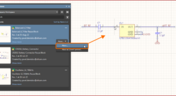
See how the Signal Analyzer by Keysight in Altium Designer lets you run signal integrity checks directly within your design environment. Read our article to learn how to effectively manage impedance, return paths, stackups, and more.

Read More
Embedded thumbnail for Enhanced Constraint Manager in Altium Designer 25. Part II: Physical Constraints and Routing Differential Pairs
Enhanced Constraint Manager in Altium Designer 25 • Jun 16, 2025
Enhanced Constraint Manager in Altium Designer 25. Part II: Physical Constraints and Routing Differential Pairs

In the second video of Samer Aldhaher’s "Enhanced Constraint Manager" series, we continue designing a 1 kW, 400 V brushless DC motor driver. This episode focuses on setting physical constraints using constraint sets, routing differential pairs, and demonstrating the Auto Shrinking feature in Altium Designer 25.

Start Watching
Embedded thumbnail for Auto-tuning Your Way to Faster PCB Design
Altium Designer's 25 Quantitative Benefits • Jun 13, 2025
Auto-tuning Your Way to Faster PCB Design

Watch how the Auto Tuning feature in Altium Designer 25 delivers optimized DDR4 routing in a single click! Fewer steps, massive time savings. Try our Benefit Calculator to estimate your own time and cost savings.

Start Watching
  • Show More
Tag (field_common_tag)
Blog • Nov 1, 2023
How to Design for Test in Embedded Systems

Whether you're designing a high-speed PCB, or a complex embedded system, it will need some level of testing. In this article, we will show you some simple tricks that can make testing and debugging a prototype much easier. 

Read More
Blog • Oct 27, 2023
Crosstalk Basics in PCB Design

Crosstalk is one of the most common issues related to electronics. Learn the basics of this phenomenon in PCB design, and gain knowledge on how to avoid it in your projects.

Read More
Blog • Oct 25, 2023
Top 3 Multi-Board PCB Connectivity Errors

Preparing complex PCB designs can often keep you awake at night. Learn more about some of the most common issues encountered in multi-board electrical connections.

Read More
Blog • Oct 23, 2023
Access to your Training Certificates on My Altium

Introduce an update on the My Altium user page that highlights your certificates and tracks your training progress, with one-click access to the Training Dashboard and Training Catalog pages. Easily view and share your certificates, keep an eye on your learning journey, and explore a variety of training resources.

Read More
Blog • Oct 19, 2023
Rigid-Flex PCBs: Advantages and Challenges

In this article, we will begin with a basic explanation of how rigid-flex technology differs from rigid board technology. We will then provide an overview of the advantages and conclude with a discussion of the challenges to be aware of.

Read More
Intrusive Soldering
Blog • Oct 17, 2023
When Should You Use Intrusive Soldering?

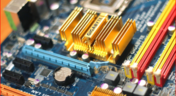
Through-hole components are frequently employed in power electronics, particularly when dealing with AC power from a wall outlet. In this article, you can delve into the intrusive soldering process and discover when it can be applied in PCB design.

Read More
multi-board-design
Blog • Oct 11, 2023
Unveiling the Crucial Role of PCB Harness Design Capabilities in Multi-Board Designs

Multi-board designs are the key to meeting evolving demands, requiring robust PCB Harness Design for seamless interconnection and success. Join us as we explore the importance of PCB Harness Design capabilities and how they are crucial for the success of multi-board designs.

Read More
We are releasing the Altium 365 BOM Manager to the public!
Blog • Oct 4, 2023
We are releasing the Altium 365 BOM Manager to the public!

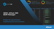
After a successful open beta phase, we're excited to release the Altium 365 BOM Manager to the market! Connect design and procurement to reduce costly design respins and improve time to market with unmatched part data insights and collaboration features from the moment the first components are placed on the schematic. Start optimizing your hardware development process today! Request your evaluation access now

Read More
Blog • Oct 2, 2023
What Makes a PCB Enclosure Rugged?

Whether you purchase products off-the-shelf or online, they all come housed within an enclosure. In some cases, these enclosures are intentionally ruggedized to withstand harsh environments or mechanical shocks. You can learn more about enclosures in this new and interesting article.

Read More
Blog • Sep 27, 2023
Concept Phase – Lid Assembly Design Part 2

We are continuing our journey through the lid assembly design phase of our Open Source Laptop project. In this section, we will discuss the layout of the test adapter and provide a demonstration of the first test for the display panel, along with the initial steps involved in assembling the boards.

Read More
Blog • Sep 20, 2023
Concept Phase – Lid Assembly Design Part 1

In the exciting next phase of the open-source laptop project we're (finally) diving into design, and getting hands-on with the display panel. Discover how we're selecting the right panel, integrating it seamlessly, and creating a custom DisplayPort adapter to illuminate the screen. Plus, learn how our choices impact features like microphones, webcams, and touch sensors, and how Altium can help bring it all to life. It’s not too late to join as we continue on this innovative journey!

Read More
Blog • Sep 7, 2023
Unleashing the Power of Concurrent PCB Design

Concurrent PCB Design is essential to unlocking the full potential of engineering teams and delivering innovative products that meet the demands of the modern world. Learn more about the main capabilities and the numerous benefits of this upcoming feature in Altium Designer.

Read More
Blog • Sep 4, 2023
Crosstalk Reduction and Elimination Techniques in Altium Designer

Whether you're designing a digital board with a ton of traces, or an RF board operating at very high frequencies, any electronic device with propagating signals will experience crosstalk. Learn more about some sure-fire ways you can reduce crosstalk in your high-speed designs.

Read More
Blog • Aug 31, 2023
Baxandall Volume Control for Audio

The Baxandall volume control is an especially useful, flexible, and simple-to-implement circuit for numerous audio designs. In this article, we will demonstrate how to design this type of equipment.

Read More
Blog • Aug 28, 2023
Common Flex Design Mistakes and How to Fix Them

Designing flexible circuits involves managing numerous factors. Discover how to prevent mistakes in this process and how to rectify them post-implementation.

Read More
Blog • Aug 24, 2023
How Much PCB Mask Expansion is Too Much?

In this article you will learn about finding the right balance between PCB mask expansion and potential problems.

Read More
  • Show More
Tag (field_common_tag)
Embedded thumbnail for How to Create and Use Impedance Profiles
How to work with Layer Stack Manager • Jul 29, 2022
How to Create and Use Impedance Profiles

Using the Altium Designer Layer Stack Manager, we will show how to create impedance profiles for transmission lines and how to apply them to the circuit board using the PCB Rules and Constraints Editor.

Start Watching
Embedded thumbnail for Creating a PCB Footprint Courtyard
How to create a PCB Footprint • Jul 27, 2022
Creating a PCB Footprint Courtyard

The courtyard is an essential piece when you want to create a PCB Footprint in Altium Designer. We’ll talk about what a courtyard is, how to create a courtyard, and how to format a courtyard correctly for your PCB footprint.

Start Watching
Embedded thumbnail for How to Edit Existing Tracks in Altium Designer
How-To's • Jul 25, 2022
How to Edit Existing Tracks in Altium Designer

This new design rule flags a violation when the creepage distance across non-conductive surface and edge regions of the board, between the targeted signals, is equal to or less than the specified Creepage distance.

Start Watching
Embedded thumbnail for Creating a PCB Footprint Silkscreen Overlay
How to create a PCB Footprint • Jul 22, 2022
Creating a PCB Footprint Silkscreen Overlay

When creating a PCB footprint in Altium Designer creating a silkscreen overlay is an important requirement. We’ll go over the standards for creating a silkscreen overlay for a footprint and the steps to creating one, such as constructing lines and measuring distance of objects and primitives.

Start Watching
Embedded thumbnail for Adding Designators for Assembly Drawings
How-To's • Jul 18, 2022
Adding Designators for Assembly Drawings

Designators for assembly drawings are added on the assembly layer. This video shows how to add the designators.

Start Watching
Embedded thumbnail for Stackup Material Library
How to work with Layer Stack Manager • Jul 15, 2022
Stackup Material Library

In this video we will learn more about the Altium designers Layer Stack Mangers built-in materials library, and how to add new material and use it in our board stack. We will also look at how we can save the user materials to an xml format.

Start Watching
Embedded thumbnail for Placing Footprint Pads
How to create a PCB Footprint • Jul 13, 2022
Placing Footprint Pads

Every footprints needs proper pad placement to ensure trace connectivity. Placing pads is the first step towards footprint creation.

Start Watching
Embedded thumbnail for Setting the Transparency for Layers and Primitives
How-To's • Jul 11, 2022
Setting the Transparency for Layers and Primitives

Customize your workspace by setting the transparency of layers and primitives in the PCB.

Start Watching
Embedded thumbnail for Create New Via Types Using the Layer Stack Manager
How to work with Layer Stack Manager • Jul 8, 2022
Create New Via Types Using the Layer Stack Manager

In this video, we will learn how to create new via types using the Layer Stack Manager, and how to create new Routing Via design rules using the PCB Rules and Constraints Editor. We will also explore how to use the different types of Via during interactive routing.

Start Watching
Embedded thumbnail for How to Create a Copper Board Report
How-To's • Jul 4, 2022
How to Create a Copper Board Report

This video will show how to create a copper board report in your PCB which can be useful for copper balance in DFM process

Start Watching
Embedded thumbnail for Stackup Creation and editing
How to work with Layer Stack Manager • Jul 1, 2022
Stackup Creation and editing

This video shows how to view and edit the PCB Layer Stack, select materials and add new layers

Start Watching
Embedded thumbnail for Configuring Your PCB Library
How to create a PCB Footprint • Jun 29, 2022
Configuring Your PCB Library

It is important to have accurate footprints to manufacture your PCB. Learn how to configure your PCB library to facilitate footprint creation.

Start Watching
Embedded thumbnail for How to Validate Links Between Components and Footprints
How-To's • Jun 27, 2022
How to Validate Links Between Components and Footprints

Before importing or updating data from the circuit to the board, you must first verify that all components of the circuit are associated with Footprint. Watch this video to learn how to validate the links between your schematic components and footprints.

Start Watching
Embedded thumbnail for How to use Copy Room Format
How to work with Rooms • Jun 24, 2022
How to use Copy Room Format

Rooms allow you to use rules on specific areas of your design. This helps immensely with properly defining trace widths and hole sizes for specific components. We’ll show you how easy it is to assign rules to specific rooms in the PCB.

Start Watching
Embedded thumbnail for How To Do Versioning And Releases by Robert Feranec and Michal Faruga
Discovering Altium 365 • Jun 20, 2022
How To Do Versioning And Releases by Robert Feranec and Michal Faruga

Meet Robert Feranec in an educational video on version control, project history, comments, comparison and other features in Altium Designer 

Start Watching
Embedded thumbnail for Using Rooms in Rules
How to work with Rooms • Jun 17, 2022
Using Rooms in Rules

Rooms allow you to use rules on specific areas of your design. This helps immensely with properly defining trace widths and hole sizes for specific components. We’ll show you how easy it is to assign rules to specific rooms in the PCB.

Start Watching
  • Show More
Tag (field_common_tag)
Why Altium Designer is Your Next Step for PCB Design
On-Demand Webinar • Oct 24, 2024
Why Altium Designer is Your Next Step for PCB Design
Join us to see how moving to Altium Designer can enable resilient and scalable designs while streamlining your entire workflow.
Watch Now
ADv25
On-Demand Webinar • Oct 24, 2024
Modernizing Engineering Workflows: Altium Designer 25 and the Future of Concurrent Design
Struggling with team misalignment and design errors? Join our exciting webinar to discover the groundbreaking advancements in Altium Designer 25!
Watch Now
KiCad Webinar
On-Demand Webinar • Oct 16, 2024
Taking the Next Step: Growing Beyond KiCad with Altium
Join our upcoming webinar to discover how Altium Designer can transition your KiCad projects without any data loss
Watch Now
Synchronize to Optimize Jira Integration
On-Demand Webinar • Oct 7, 2024
Synchronize to Optimize: Enhancing Efficiency with Jira Integration for Altium 365
Tired of juggling multiple tools for project management? Watch the webinar and see how Jira Integration for Altium 365 can optimize your workflows.
Watch Now
Wire bonding
On-Demand Webinar • Sep 29, 2024
Unlock New Design Possibilities with Wire Bonding
Explore how wire bonding can enhance your designs, provide size reduction, improve power management, and increase mechanical reliability.
Watch Now
routing
On-Demand Webinar • Sep 29, 2024
Advanced Routing Features & Techniques
To help you get the most out of your experience with Altium Designer, join our webinar this month and learn advanced routing techniques.
Watch Now
signal analyzer
On-Demand Webinar • Sep 25, 2024
Signal Integrity Made Simple
Discover how to easily detect and resolve high-speed signal integrity challenges without the need for extensive expertise.
Watch Now
competitive-displacement-webinar-3
On-Demand Webinar • Sep 20, 2024
Mastering Design Complexity: How Altium Designer Outperforms Cadence in Solving Workflow and Engineering Challenges - Part 2
Join our webinar to learn how to enhance efficiency, foster better collaboration, and accelerate your time-to-market with Altium unified solutions.
Watch Now
Breaking Down Silos Webinar
On-Demand Webinar • Sep 16, 2024
Breaking Down Data Silos: A Practical Comparison of Altium and Cadence in Cross-Functional PCB Design
Join us for a webinar that addresses the critical challenges of maintaining design data continuity across various design functions.
Watch Now
Draftsman
On-Demand Webinar • Sep 10, 2024
Mastering Design Complexity: How Altium Designer Outperforms Cadence in Solving Workflow and Engineering Challenges
Join our upcoming webinar to discover why engineers consistently choose Altium Designer as the standard in PCB design.
Watch Now
SPICE
On-Demand Webinar • Sep 3, 2024
Mastering SPICE Simulation in Altium Designer
Discover how the SPICE engine in Altium Designer can help you easily verify that your finished project functions as intended.
Watch Now
Output job
On-Demand Webinar • Aug 24, 2024
Beyond PCB Design with Altium Designer
In this webinar we'll dive into the essential aspects that go beyond the schematic and layout.
Watch Now
PCB
On-Demand Webinar • Aug 23, 2024
Elevate Your Design Skills: Tips & Tricks for Success
Discover practical insights and efficient methods that can enhance your PCB design capabilities.
Watch Now
Cyber Security Webinar Cover
On-Demand Webinar • Aug 6, 2024
The Anatomy of IT Compliance in Electronics Development: Altium 365 & AWS GovCloud
Are you an IT or security professional looking for a secure electronics design collaboration platform that could also support your ITAR and EAR compliance efforts? If so, watch this webinar to bring together the expertise of Altium 365 and AWS!
Watch Now
Design reuse
On-Demand Webinar • Aug 1, 2024
How to Speed-up Product Development with Reusable Circuitry
In this webinar you'll learn more about the benefits of the design reuse blocks approach as well as the Design Reuse panel.
Watch Now
Harness design
On-Demand Webinar • Jul 19, 2024
Stay Ahead of the Curve: A Half-Year Review of Altium Designer Improvements
Join our exciting webinar to discover the groundbreaking advancements in Altium Designer!
Watch Now
  • Show More
Tag (field_common_tag)
Loading
Loading...
Share link
Share with
Search by Update
Version
Update
25 26 24 23 22
25.0 25.1 25.2 25.3 25.4 25.5 25.6 25.7 25.8 25.9
26.1 26.2
24.10 24.9 24.8 24.7 24.6 24.5 24.4 24.3 24.2 24.1 24.0
23.11 23.10 23.9 23.8 23.7 23.6 23.5 23.4 23.3 23.2 23.1 23.0
22.11 22.10 22.9 22.8 22.7 22.6 22.5 22.4 22.3