
Main navigation

  • Home
  • Discover
  • Learning Center
  • What’s New

Second main navigation

  • Altium Community
  • Support
  • Documentation
×

Results

  • Updates
  • Blog 570
  • Video 540
  • Webinar 86
  • Playlist 53
Filters:
Tag (field_common_tag)
Blog • Jul 9, 2025
How to Make Your PCB Layout AOI and X-Ray Friendly

Designing for inspection is key to reliable manufacturing. This article covers practical PCB layout tips to optimize your board for AOI and X-ray inspection helping you reduce defects, false positives, and production delays.

Read More
Embedded thumbnail for How Close Can You Bring a Reference Plane?
How-To's • Jul 8, 2025
How Close Can You Bring a Reference Plane?

Explore our in-depth investigation into practical simulations using both Altium Designer and Polar Si9000. We demonstrate impedance sensitivity analysis and reveal the real limitations of optimizing reference plane proximity for improved signal shielding.

Start Watching
Blog • Jul 7, 2025
Understanding Systems Engineering

Read our brand-new article where we explore the key areas of an engineering project and the different stages of electronic product development from a project execution perspective. From initiation and planning to design, development, validation, testing, and certification, we walk you through each phase to help you understand how successful electronic products are brought to life.

Read More
Embedded thumbnail for Do PCB Thermal Vias Actually Work?
How-To's • Jul 3, 2025
Do PCB Thermal Vias Actually Work?

Are thermal vias really helping your PCB’s heat management? Tech Consultant Zach Peterson dives into simulation data, research, and a controversial article to uncover the truth. Learn why via count and spacing matter more than sheer quantity.

Start Watching
Blog • Jul 2, 2025
PCB First-Pass Yield: Small Decisions That Make a Big Difference

This article highlights how seemingly minor layout choices like trace spacing, component footprints, or stack-up details can dramatically impact whether a board passes fabrication and assembly the first time.

Read More
Blog • Jul 1, 2025
Implementing Design for Supply Chain Principles in Electronic Product Development

Designing with supply chain principles in mind helps you avoid delays, reduce costs, and ensure manufacturability. This article outlines practical strategies for component selection, sourcing, and lifecycle management to make your designs more resilient and production-ready.

Read More
Embedded thumbnail for Stripline Routing Deep Dive: How Close Is Too Close?
How-To's • Jun 30, 2025
Stripline Routing Deep Dive: How Close Is Too Close?

In this video, Zach Peterson takes a deep dive into what happens when reference layers are incorrectly set in a PCB stackup and how that affects impedance, signal integrity, and EMC. He also shares valuable insights into stripline routing proximity issues and best practices for assigning reference planes.

Start Watching
Blog • Jun 27, 2025
Beyond the BOM: How Proactive Component Selection Is Transforming Workflows

Learn how proactive component selection helps you avoid supply chain risks, reduce costs, and design more reliably. Our new article outlines key strategies and shows how tools like Altium 365 support smarter part decisions.

Read More
Blog • Jun 26, 2025
Power Integrity Issues?

Power problems can be hard to spot until it’s too late. See how easy it is to analyze your power nets, check voltage drops, and improve reliability with Power Analyzer by Keysight - all without leaving your design environment.

Read More
Embedded thumbnail for Coming Soon: Solder Mask Zero Expansion
New in Altium Designer 25 • Jun 25, 2025
Coming Soon: Solder Mask Zero Expansion

Solder Mask Zero Expansion marks a move toward industry alignment, specifically with IPC-7351B and IPC-2581B standards. It changes the default solder mask expansion value from 4 mil to 0 mil. Discover more upcoming updates on our Coming Soon Page.

Start Watching
Blog • Jun 24, 2025
How to Design High-Speed PCBs Without Signal Surprises

Signal issues can sneak in early and cost you later. Read our whitepaper to see how Signal Analyzer by Keysight (inside Altium Designer) helps you catch problems fast and design with confidence.

Read More
Embedded thumbnail for Analog Supply without a Ferrite: Proper Isolation Techniques Explained
How-To's • Jun 20, 2025
Analog Supply without a Ferrite: Proper Isolation Techniques Explained

In our new tutorial, you'll learn why ferrite beads may not be the best choice for isolating analog and digital supply pins on integrated circuits. Zach Peterson debunks common misconceptions about ferrite bead isolation and introduces better alternatives, including dedicated LDOs, precision voltage references, and effective filtering techniques to help you achieve cleaner analog signals in your designs.

Start Watching
Blog • Jun 18, 2025
Beyond Basic Part Selection: Using Supply Chain Data to Validate Choices

Learn how to enhance part selection by using real-time supply chain data. This article shows how integrating insights like availability and lifecycle status helps you make smarter, risk-aware design choices.

Read More
Blog • Jun 17, 2025
Signal Mistakes Are Expensive

See how the Signal Analyzer by Keysight in Altium Designer lets you run signal integrity checks directly within your design environment. Read our article to learn how to effectively manage impedance, return paths, stackups, and more.

Read More
Embedded thumbnail for Enhanced Constraint Manager in Altium Designer 25. Part II: Physical Constraints and Routing Differential Pairs
Enhanced Constraint Manager in Altium Designer 25 • Jun 16, 2025
Enhanced Constraint Manager in Altium Designer 25. Part II: Physical Constraints and Routing Differential Pairs

In the second video of Samer Aldhaher’s "Enhanced Constraint Manager" series, we continue designing a 1 kW, 400 V brushless DC motor driver. This episode focuses on setting physical constraints using constraint sets, routing differential pairs, and demonstrating the Auto Shrinking feature in Altium Designer 25.

Start Watching
Embedded thumbnail for Auto-tuning Your Way to Faster PCB Design
Altium Designer's 25 Quantitative Benefits • Jun 13, 2025
Auto-tuning Your Way to Faster PCB Design

Watch how the Auto Tuning feature in Altium Designer 25 delivers optimized DDR4 routing in a single click! Fewer steps, massive time savings. Try our Benefit Calculator to estimate your own time and cost savings.

Start Watching
  • Show More
Tag (field_common_tag)
Blog • Oct 22, 2025
Bridging Mechanical and Electrical Teams for Smarter Automotive Design

As vehicles evolve into advanced electronic systems, the separation between electrical and mechanical design teams becomes a critical bottleneck. This article explores how synchronized ECAD–MCAD workflows help automotive projects move faster, reduce rework and maintain design integrity.

Read More
Blog • Oct 20, 2025
Via Structures: Designing for Reliability, Not Just Density

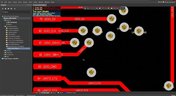
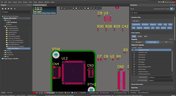
We all want to pack more into our PCB designs, but the smallest via isn’t always the smartest one. Dive in to learn how picking the right structure can save you headaches down the line.

Read More
Blog • Oct 15, 2025
How Structural Electronics Enables 3D, Flexible, and Wearable Integration

Structural electronics integrates electronic functionality directly into the physical structure of a product, eliminating the need for traditional circuit boards. This article examines how advances in materials, additive manufacturing, and flexible substrates are enabling compact, 3D, and wearable systems with enhanced performance and design freedom.

Read More
Blog • Oct 9, 2025
Beyond Traces: Why Soldermask May Be the Critical Factor in Ultra HDI

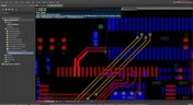
In ultra-HDI designs, soldermask is no longer a passive coating but a pivotal element that can determine manufacturability. This article explores why mask registration, resolution, and feature tolerances become critical as line spacings shrink below 50 µm.

Read More
Blog • Oct 7, 2025
How ECAD-MCAD Co-Design Supports Aerospace Reliability and Compliance

When the margin for error is nearly zero, aerospace engineering demands a design process that’s seamless across all domains. Here, we explore how ECAD-MCAD co-design delivers an integrated workflow that supports first-pass success and compliance with strict aerospace standards.

Read More
Blog • Oct 2, 2025
Most Common Causes of PCB Assembly Rework and Scrap

Many PCB assemblies fail not because of exotic faults, but due to basic issues like incorrect BOM entries or footprint mismatches that force rework or scrap. This article dives into the most common causes and how to prevent costly defects in your design-to-manufacturing process.

Read More
Blog • Sep 30, 2025
Behind the Scenes with AI Embedded Development

Forget one-shot AI hacks Ari Mahpour shows the thoughtful, sustainable way to integrate AI into embedded firmware development. Learn the core principles (planning gate, HAL abstraction, observability, timeout design) that can help you push your efficiency 5-10 times in real hardware projects.

Read More
Blog • Sep 25, 2025
We're heading to PCB West 2025!

Join Altium at PCB West 2025 in Santa Clara, CA, on October 1! Stop by Booth 300 for the official launch of the new Altium platform, built on the foundation of Altium Designer and Altium 365. Be sure to check out our live demos of Altium Develop and Altium Agile.

Read More
Blog • Sep 24, 2025
Peak Electrical Performance in Multi-Board Designs With Advanced Simulation and Compliance Tools

Moving from single-board to multi-board systems is a leap in complexity. You must manage not just routing, but power, signal integrity, mechanical fit, and regulatory requirements across boards. In this article, you’ll discover how Altium’s advanced simulation and compliance tools help engineering teams overcome these challenges and deliver reliable multi-board solutions.

Read More
Blog • Sep 22, 2025
How to Catch Enclosure and Connector Misalignment Before the First Prototype

As electronics continue to miniaturize and functionality increases, even minor misalignments between enclosures and connectors can derail a project. This article explores how early integration of ECAD and MCAD workflows helps detect and eliminate those costly issues before the first prototype is built.

Read More
Blog • Sep 17, 2025
Executive Insights Into Electronic Product Development Gaps You Need To Close

Electronics hardware development is falling behind broader product development disciplines due to fragmented workflows, poor collaboration, and limited compliance visibility. This gap introduces risk, delays, and missed opportunities but executives see real business value in modernizing electronics development through better integration, traceability, and lifecycle visibility.

Read More
Blog • Sep 15, 2025
Sourcing For High-Mix Low-Volume Electronics Manufacturing

High-mix, low-volume (HMLV) electronics manufacturing requires agile sourcing strategies to handle shifting BOMs, erratic lead times, and component volatility. All while controlling costs and ensuring compliance. Cloud-based tools like Altium provide real-time component visibility, BOM collaboration, and supplier integrations to help navigate HMLV complexities.

Read More
Blog • Sep 10, 2025
How to Solve Fit, Form, and Function Challenges in Robotics with ECAD-MCAD Collaboration

As robotics systems become increasingly miniaturized and intricate, ensuring perfect fit, form, and function across electrical and mechanical domains is critical to avoid design setbacks. Real-time ECAD-MCAD integration with two-way sync empowers teams to streamline workflows, reduce PCB rework, and deliver more reliable designs faster.

Read More
Blog • Sep 8, 2025
One Vision, Three Powerful Solutions: Introducing Altium Discover, Altium Develop, and Altium Agile

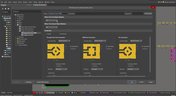
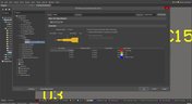
We are excited to announce the launch of three new platform-based solutions that will transform the way electronic products are designed, built, and delivered: Altium Discover, Altium Develop, and Altium Agile. These solutions are designed to simplify processes, accelerate innovation, and make collaboration seamless across the entire electronics lifecycle. Together, they realize the purpose of Altium and Renesas: To Make Our Lives Easier.

Read More
Blog • Sep 4, 2025
The Cost of Overreaction: How Misguided Orders Disrupt the Semiconductor Market

Discover how short-sighted ordering practices fuel volatility in the semiconductor market and why smarter, data-driven approaches are key to building resilience and sustainability.

Read More
Blog • Sep 2, 2025
The Top 5 Workflow Bottlenecks Slowing Down Mechanical Engineering Teams

Mechanical engineering teams frequently encounter delays from fragmented communication, disconnected toolchains, and inefficient synchronization processes. This article examines five critical workflow bottlenecks and highlights how ECAD-MCAD integration with real-time, bidirectional updates can eliminate rework and accelerate design iterations.

Read More
  • Show More
Tag (field_common_tag)
Embedded thumbnail for Searching for Errors
• Jun 16, 2020
Searching for Errors

We’ve looked at how to set up the Design Rule Checker to help us analyze our PCB design errors. Now it’s time to resolve these errors and prep our design to start generating output files.

Start Watching
Embedded thumbnail for Performing Board DRC
• Jun 16, 2020
Performing Board DRC

Design rules are crucial to a PCB’s overall design and performance. It’s just as important to adhere to these rules and ensure that we didn’t overlook any unconnected nets or short circuits. This is why we need to run a Design Rule check.

Start Watching
Embedded thumbnail for Placing a Custom 3D Body in 3D View
• Jun 16, 2020
Placing a Custom 3D Body in 3D View

With the help of the 3D view, it is possible to view a PCB design from all sides, to check on component placement, silkscreen alignment, and many other visual aspects.

Start Watching
Embedded thumbnail for Silkscreen Placement
• Jun 16, 2020
Silkscreen Placement

The silkscreen layer is the layer on which we print any visual text or symbols on our PCB. With the help of this silkscreen layer, we can print our component designators, pin placement, and more.

Start Watching
Embedded thumbnail for Working with Polygon Pours
• Jun 16, 2020
Working with Polygon Pours

When working with common signals, the current levels are usually quite minimal, but when working with power nets it’s not uncommon to see current levels of a few amps. One of the reasons to use polygons is to maintain the quality and reliability of the power supply system.

Start Watching
Embedded thumbnail for Routing Post Processes
• Jun 16, 2020
Routing Post Processes

Depending on how you routed your board, it may be a time-consuming process to fix these manually. So we’ll dive into Route Glossing a little more, along with an automated way to retrace pre-existing routes.

Start Watching
Embedded thumbnail for PCB Layout Cleanup
• Jun 16, 2020
PCB Layout Cleanup

After the board has been routed, it’s almost certain that you’ll need to either move, delete, or adjust some traces. We’ll be looking at a few basic methods to easily modify and remove traces in our design.

Start Watching
Embedded thumbnail for Differential Pair Routing
• Jun 16, 2020
Differential Pair Routing

Routing Differential Pairs is similar to routing single traces, but there are additional rules and guidelines to follow that will help you avoid signal integrity problems.

Start Watching
Embedded thumbnail for Introduction to Routing
• Jun 16, 2020
Introduction to Routing

We’ve looked at different routing behaviors and options that we can change to make routing much easier. So we’re going to dive into the basics of routing and how these settings and routing modes can be applied.

Start Watching
Embedded thumbnail for Defining the Layer Stackup
• Jun 10, 2020
Defining the Layer Stackup

The PCB is designed and formed as a stack of layers and the definition of the PCB layer stack is a critical element of successful printed circuit board design. In Altium Designer, the Layer Stack Manager is used to develop the printed circuit board internal design including layer-pairing, careful via design, any back drilling requirements, rigid/flex requirements, copper balancing, layer stack symmetry, and material compliance. This video guides you through creation of a layer stackup, adding the necessary layers, as well as adding an impedance profile.

Start Watching
Embedded thumbnail for Searching for Errors in Schematic
• May 20, 2020
Searching for Errors in Schematic

Searching for Errors: Errors and mistakes happen to everyone - from beginners to professionals. So we always preach how it is paramount for your design to be validated before pushing it to the PCB. But luckily it’s pretty easy to find and analyze any errors using Altium Designer. We’ll take a look at how to find and analyze errors in your schematic.

Start Watching
Embedded thumbnail for Creating Net Classes
• Jun 2, 2020
Creating Net Classes

A Net Class is a collection of nets that can be used for creating a targeted design rule. So for example, you may want all power and ground nets to have a minimum track width to handle a specific current rating. So we’ll show you how to assign these nets to a NetClass. 

Start Watching
Embedded thumbnail for Configuring Design Rules - Part 2
• May 14, 2020
Configuring Design Rules - Part 2

Altium Designer uses the concept of Design Rules to define the requirements of a design. These rules collectively form an instruction set for the PCB Editor to follow. They cover every aspect of the design - from routing widths, clearances, plane connection styles and so on. With a well-defined set of design rules, you can successfully complete board designs with varying and often stringent design requirements.

Start Watching
Embedded thumbnail for Routing Modes and Setup
• May 12, 2020
Routing Modes and Setup

Most of you know that routing can be a time consuming process, but it doesn’t have to be a daunting task if you have the right tools. So we’ll be looking at what options and settings can help us perfect the art of routing.

Start Watching
Embedded thumbnail for PCB Component Placement
• May 12, 2020
PCB Component Placement

Component placement in the PCB is an important stage of the design process as it sets the precedent for efficient and clean routing. We’ll be diving into different component placement methods along with some tips and tricks that you can use to make this an easy process. 

Start Watching
Embedded thumbnail for Configuring the Basic Rules
• May 12, 2020
Configuring the Basic Rules

Altium Designer uses the concept of Design Rules to define the requirements of a design. These rules collectively form an instruction set for the PCB Editor to follow. They cover every aspect of the design - from routing widths, clearances, plane connection styles and so on. With a well-defined set of design rules, you can successfully complete board designs with varying and often stringent design requirements.

Start Watching
  • Show More
Tag (field_common_tag)
BOM Editor
On-Demand Webinar • Jun 13, 2024
BOM Editor
Watch Now
Simulation
On-Demand Webinar • May 24, 2024
The Value of Upgrading: Time and Financial Advantages of Recent Altium Versions
Learn how features such as PCB Layout Replication, Auto Tuning, and Simulation are making design processes more efficient and effective.
Watch Now
Constraint Manager
On-Demand Webinar • May 22, 2024
Constraint Manager
Watch Now
Configurable Workflows In-App On Demand
On-Demand Webinar • May 20, 2024
Configuring Electronics Development Workflows That Really Work: Best Practices
Watch the webinar to understand the impact of disjointed workflows on project timelines, product quality, and cross-functional collaboration. Learn how configurable workflows can help you accelerate innovation and maintain competitive advantage.
Watch Now
Iterate Faster in Complex Engineering Projects Webinar Cover
On-Demand Webinar • May 15, 2024
Iterate Faster in Complex Engineering Projects
Learn how Valispace is transforming the world of requirements and systems engineering, enabling teams to do super fast design iterations and develop quality products while ensuring they comply with standards and regulations.
Watch Now
Z2Data Webinar Cover
On-Demand Webinar • Apr 25, 2024
Bridge the Information Divide: Altium 365 Meets Z2Data
Watch the webinar to learn how Z2Data can help you build resilience in engineering, compliance, and procurement through the comprehensive supply chain and component data.
Watch Now
Data management
On-Demand Webinar • Apr 22, 2024
Mastering Data Management with Altium Designer 24
Join our webinar to learn how easy it is to manage, access, and synchronize your data with Altium Designer 24.
Watch Now
BOM Portal Webinar Cover
On-Demand Webinar • Apr 19, 2024
Bridge the Gap Between Engineering and Procurement: Altium 365 BOM Portal
Watch the webinar to learn how to make informed decisions and mitigate supply chain risks with Altium 365 BOM Portal, BOM management application purpose-built for electronics engineering and procurement. Improve your time to market and proactively manage electronic component supply chain risks.
Watch Now
Enterprise Subscription
On-Demand Webinar • Apr 18, 2024
Introduction to Altium 365 Enterprise Subscription Level
Watch Now
Introduction to Altium 365 Enteroruse Subscription
On-Demand Webinar • Apr 18, 2024
Introduction to Altium 365 Enterprise Subscription Level
Watch Now
AD Subscription levels
On-Demand Webinar • Apr 18, 2024
Introduction to Altium 365 Pro Subscription
Watch Now
Altium 365 Standard Subscription
On-Demand Webinar • Apr 18, 2024
Introduction to A365 Subscription Levels - Standard
Watch Now
Harness Design
On-Demand Webinar • Apr 18, 2024
Harness Design Introductory Demo
In this video, we explore Altium Designer's integrated harness design features, showing how it simplifies creating wiring harnesses within the same environment as PCB and system design.
Watch Now
Introduction to Altium Designer Subscription Levels
On-Demand Webinar • Apr 18, 2024
Introduction to Altium Designer Subscription Levels
Whether customer designs are simple or complex, and your customers work solo or in a team,
Altium has a solution for every engineer or enterprise. Altium offers three subscription levels, Standard, Pro and Enterprise.
Watch Now
MCAD CoDesigner
On-Demand Webinar • Apr 18, 2024
MCAD CoDesigner: ECAD-MCAD Collaboration
This video introduces the MCAD CoDesigner feature in Altium Designer, a powerful tool designed to enhance collaboration between electrical and mechanical engineers.
Watch Now
SiliconExpert Integration Altium 365
On-Demand Webinar • Apr 11, 2024
Design with Confidence: Altium 365 Meets SiliconExpert
Watch the webinar to learn how SiliconExpert Integration in Altium 365 can optimize your workflows and elevate your design process.
Watch Now
  • Show More
Tag (field_common_tag)
Loading
Loading...
Share link
Share with
Search by Update
Version
Update
25 26 24 23 22
25.0 25.1 25.2 25.3 25.4 25.5 25.6 25.7 25.8 25.9
26.1 26.2
24.10 24.9 24.8 24.7 24.6 24.5 24.4 24.3 24.2 24.1 24.0
23.11 23.10 23.9 23.8 23.7 23.6 23.5 23.4 23.3 23.2 23.1 23.0
22.11 22.10 22.9 22.8 22.7 22.6 22.5 22.4 22.3