
Main navigation

  • Home
  • Discover
  • Learning Center
  • What’s New

Second main navigation

  • Altium Community
  • Support
  • Documentation
×

Results

  • Updates
  • Blog 571
  • Video 541
  • Webinar 86
  • Playlist 53
Filters:
Tag (field_common_tag)
Blog • Aug 11, 2025
Getting Started with the GreenPAK Introduction Kit

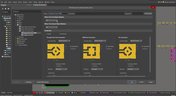
Take your first steps into mixed-signal design with the Renesas GreenPAK Introduction Kit. Ari Mahpour shows how to design, simulate, and validate a clock divider project, making it easy for beginners to start experimenting with programmable mixed-signal devices.

Read More
Embedded thumbnail for Arduino to Custom PCB: Professional Design Transformation
How-To's • Aug 7, 2025
Arduino to Custom PCB: Professional Design Transformation

Discover how to upgrade your Arduino Nano-based PCB design into a professional, custom PCB. This tutorial walks through the process of replacing development boards with individual components to create a production-ready design, using a real drone project as the example.

Start Watching
Blog • Aug 6, 2025
Smarter Electronic Part Sourcing for Automotive Purchasing Professionals

Targeted at procurement professionals in the automotive industry, the article outlines the evolving pressures of sourcing components for electrified and connected vehicles. It highlights Octopart’s ecosystem as a unified tool that centralizes availability, compliance, pricing, and lifecycle intelligence to optimize sourcing efficiency.

Read More
Embedded thumbnail for PCB Library Management: One Library or Many?
How-To's • Aug 5, 2025
PCB Library Management: One Library or Many?

This detailed guide walks you through the pros and cons of each approach and offers proven strategies for managing component data, whether you're an independent designer or overseeing libraries for an entire organization.

Start Watching
Blog • Aug 4, 2025
Stack-Up to Success: Avoid the Pitfalls

"Stack‑Up to Success" highlights how a carefully planned PCB stack‑up is foundational to preventing warpage, managing impedance, and avoiding manufacturing delays by clearly communicating layer construction, materials, and tolerance requirements to fabricators.

Read More
Embedded thumbnail for Coming Soon: Sawtooth Rounding Support for Length Tuning
New in Altium Designer 25 • Jul 31, 2025
Coming Soon: Sawtooth Rounding Support for Length Tuning

Sawtooth Rounding for Length Tuning improves signal‑path accuracy by applying controlled corner‑rounding to sawtooth geometries during both Interactive Length Tuning and within‑pair matching in the Auto Tuning engine. Discover this capability and additional innovations on our Coming Soon page.

Start Watching
Blog • Jul 30, 2025
IC Components Explained: A Comprehensive Guide to Integrated Circuits

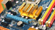
Gain a clear understanding of the fundamental elements within integrated circuits. This guide examines their structure, function, and role in system performance, knowledge that’s vital for anyone involved in sourcing or developing electronic designs.

Read More
Embedded thumbnail for Coming Soon: Z-Axis Clearance Rule
New in Altium Designer 25 • Jul 29, 2025
Coming Soon: Z-Axis Clearance Rule

The Z-Axis Clearance Rule checks the shortest distance between copper features on different layers in a PCB design. It is available in both the Constraint Manager and the legacy PCB Rules Editor. Discover more new features in Altium on our Coming Soon Page.

Start Watching
Blog • Jul 28, 2025
Ensuring Precise Connector Alignment in Multi‑Board Manufacturing

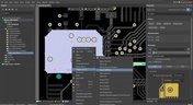
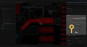
Misaligned connectors can cause major issues in multi-board assemblies. In this article, David Marrakchi shows how Altium’s 3D tools help detect and fix alignment problems early in the design process.

Read More
Embedded thumbnail for Coming Soon: Advanced Polygon Pour Engine
New in Altium Designer 25 • Jul 24, 2025
Coming Soon: Advanced Polygon Pour Engine

Now supports true arcs instead of approximated curves in copper pours. This enhanced engine marks a major advancement in the polygon pour process in Altium Designer, delivering smoother and more accurate copper shapes. Native arc rendering improves visual quality and helps ensure cleaner, more professional PCB designs.

Start Watching
Blog • Jul 23, 2025
Getting Started with the Renesas RA8D1 Evaluation Kit and Edge AI

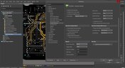
Dive into the power of Renesas’ RA8D1 MCU using the EK‑RA8D1 evaluation kit. Learn how to train, test, and deploy image‑based detection models seamlessly with Edge Impulse, and kickstart your embedded vision AI projects in minutes.

Read More
Embedded thumbnail for How to Design Rigid-Flex PCB Stackups from Scratch
How-To's • Jul 22, 2025
How to Design Rigid-Flex PCB Stackups from Scratch

Watch this tutorial to learn the fundamentals of Rigid-Flex design. We cover everything from understanding polyimide materials and adhesive layers to building complex, multi-layer Rigid-Flex constructions that are ready for manufacturing.

Start Watching
Blog • Jul 21, 2025
How to Effectively Use Jira for Hardware Development Projects

Originally built for software development, Jira has become a popular tool for agile project management across various industries. Our new article explores how hardware teams can leverage core Jira features and adapt agile principles to suit the unique needs of hardware development.

Read More
Embedded thumbnail for How to Draw Antipads - Complete Tutorial
How-To's • Jul 17, 2025
How to Draw Antipads - Complete Tutorial

Discover how to draw and define antipads in Altium with this complete tutorial. Learn three different methods for creating antipads around vias. From simple design rules to advanced polygon cutouts for both basic and complex PCB designs.

Start Watching
Blog • Jul 16, 2025
Building Supply Chain Resilience: Transforming BOM Management for Modern Electronics

Discover why top electronics companies are replacing spreadsheets with purpose-built BOM management solutions. This whitepaper outlines the risks of outdated methods, offers a readiness checklist, and explores how BOM Portal helps teams cut costs, reduce risk, and speed up development with smarter, data-driven workflows.

Read More
Embedded thumbnail for Do PCB Manufacturers Actually Look at Fabrication Drawings?
How-To's • Jul 15, 2025
Do PCB Manufacturers Actually Look at Fabrication Drawings?

Explore this in-depth tutorial featuring real fabrication drawings, stackup specifications, and drill tables - all created using Altium Designer’s Draftsman tool. Learn essential insights into PCB data management and manufacturing requirements from an industry perspective.

Start Watching
  • Show More
Tag (field_common_tag)
Article preview
Blog • Sep 8, 2020
Sharing PCB Data with Manufacturers in the Cloud

Once you’ve finished your new project and you’re ready to push it to your manufacturer, you’ll normally be stuck in an endless email chain with an engineer, or you’ll have to share cloud links with each other. The cloud sharing and design release tools in Altium Designer and Altium Concord Pro are a huge help in this area. In this post, I’m going to take an existing project I’ve worked with in a number of recent blogs, create some fabrication and assembly documentation, and finally push this data to a manufacturer using Altium Concord Pro.

Read More
Article preview
Blog • Sep 3, 2020
The Great PCB Layout "Rules of Thumb" Debate Rages On

To this day, I still see many PCB layout “rules of thumb” that first became common nearly 20 years ago. Do these rules still universally apply? The answer is a firm “maybe.” The discussion around PCB layout rules of thumb is not that these rules are correct or incorrect. The problem is that the discussion around these rules often lacks context, leading to the always/never type of discussion seen in some popular forums. My goal in this article is to communicate the context behind the common PCB design rules.

Read More
Article preview
Blog • Sep 1, 2020
How to Design Your PCB Test Coupon and What You Can Test

As the operating speed of components has increased, controlled impedance is becoming more common in digital, analog, and mixed-signal systems. If the controlled impedance value for an interconnect is incorrect, it can be very difficult to identify this problem during an in-circuit test. However, testing is normally performed on a PCB test coupon, which is manufactured on the same panel as the PCB. If you want to get through board spins quickly and aid future designs, you might consider designing a test coupon and keeping it handy for future designs.

Read More
Article preview
Blog • Aug 20, 2020
Altium DbLibs and Electronic Components in the Cloud with Altium Designer 20.1

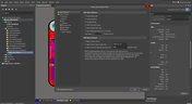
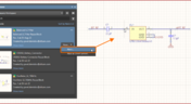
Altium’s DbLib support is one of the oldest and most loved features of Altium Designer for managing electronic components and their data. They’ve been present in the software world since before I could fathom the existence of Ohm’s law. Altium 20.1’s new Component Sync feature allows you to synchronize virtually any database or database Library with Altium 365, taking advantage of both approaches strengths.

Read More
Article preview
Blog • Aug 18, 2020
What is a Schematic Netlist for Your PCB?

If you’ve created your next great schematic, there is a lot going on behind the scenes in your design software. A schematic netlist is one of the central pieces of information that will be used in multiple features in your design software to create a real PCB. Your schematic netlist provides both electrical connectivity information, and reflects the functional structure of your design data in a single set of data.

Read More
Article preview
Blog • Aug 13, 2020
How to Select an Inductor for a Buck Converter

An SMPS is one of those quiet (yet electrically noisy) devices that makes your favorite electronics run smoothly. Among the numerous DC-DC converter topologies, a buck converter finds plenty of uses for stepping down the input voltage to a lower level while providing high efficiency power conversion. A common question around component selection for these power converters is how to select an inductor for a buck converter. The goal in working with an inductor and other components in a buck converter is to limit power loss to heat and while minimizing current ripple.

Read More
Article preview
Blog • Aug 11, 2020
US Department of Transportation Seeking Alternatives to GPS

GPS-capable devices range from your phone to your smartwatch; simply type in your destination and follow the directions. Simple, right? According to the Washington Post, we should all stop using GPS as it’s ruining the navigation centers of our brains. Despite the neurological effects on perception and judgment, the U.S. Department of Transportation (DOT) aims to find alternatives to GPS to provide redundancy.

Read More
Article preview
Blog • Aug 6, 2020
Bluetooth 5.1 SoC vs. Module: Which is Best for Your Design?

The list of features available in Bluetooth just got a little longer since the release of Bluetooth 5.1. If you want to incorporate a Bluetooth 5.1 SoC into your new product, you have two primary options for bringing this component into your board. The first is as an SoC that mounts to your board just like any other component. The other option is to bring a module into your new board—directly onto the surface layer. Here’s what you need to know about a Bluetooth 5.1 SoC or module in your next IoT product.

Read More
Altium 365 Getting Started User Guide - Available Now
Blog • Aug 5, 2020
Altium 365 Getting Started User Guide - Available Now

Get Started with Altium 365 with a step-by-step guide and videos to experience the most connected experience for PCB design and realization: https://my.altium.com/altium-365/getting-started/

Read More
Article preview
Blog • Aug 4, 2020
USB Power Delivery for Your Next Project

Since its introduction in the late 90s, the USB standard has never ceased to grow in popularity. There has been a growing trend toward USB being a power delivery interface with data, rather than a data interface that can supply power, as the 1.0 specification originally intended. To supply the increasing thirst for power over USB, the USB 3.0 Spec with Type-C began implementing the Power Delivery standard, which you should consider using for your next electronics project.

Read More
Article preview
Blog • Jul 30, 2020
Circuit Board Design for In-Circuit Testing

There are many types of circuit board tests available in electronics manufacturing today, each having unique goals and characteristics. This article presents guidelines at the design level (schematic and layout) to enable the use of in-circuit testing (ICT) fixtures to verify proper component assembly. These simple test fixtures allow your board to be tested as its assembled, which helps identify and remove failed boards from your production run.

Read More
Article preview
Blog • Jul 28, 2020
Planning for the Future with Cirris Systems and Altium

Technological advancements have been a hallmark of the past few decades, from the widespread adoption of internet technology to the smartphones and wireless devices we rely on every day to stay connected. Orlan Thatcher, Board Layout Specialist at Cirris Systems, could never have predicted the demand their services would generate. The company struggled with six different software platforms before switching to Altium Designer.

Read More
Article preview
Blog • Jul 23, 2020
An Introduction to NFC

I used to work in a research lab that worked primarily with RFID (Radio Frequency IDentification) and NFC (Near Field Communication) technology, particularly for the agriculture industry and cattle identification. These were very specialized fields; however, the lab also worked on projects which involved retail and various other applications for NFC. It’s an amazing technology that you might be using every day without thinking about it - building access to your mobile phone payments, for instance. 

Read More
Article preview
Blog • Jul 22, 2020
Editing Your PCB Geometry with MCAD Tools

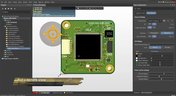
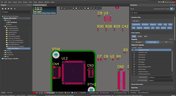
You need to define your PCB geometry in the context of your enclosure. If your board cannot physically be assembled into the final product, it doesn't matter how well laid out it is electrically. This webinar focuses on how the MCAD CoDesigner allows you to edit your PCB in the context of a higher-level assembly, allowing you to respect the relevant mechanical constraints.

Read More
Blog • Jul 21, 2020
The PCB Fabrication Process — what Every Design Engineer Needs To Know, Part 2

In Part 1 of this article, I described the first steps that occur during the PCB fabrication process. They detailed the inner layer processing effort as well as the efforts that take place during the transition from inner layer processing to lamination. This part of the article will provide a detailed description of the lamination, drilling and plating processes.

Read More
Blog • Jul 16, 2020
The PCB Fabrication Process—What Every Design Engineer Needs To Know, Part 1

There are still a number of designers - perhaps most of them - who have never toured a PCB fabrication facility. They are also unaware of the various steps that occur during the fabrication process. The purpose of this article is to describe those steps and what transpires in each of them. Part 1 of this article focuses on inner layer processing and the steps that are done prior the lamination process.

Read More
  • Show More
Tag (field_common_tag)
Embedded thumbnail for Resolving Errors in the PCB
• Jun 17, 2020
Resolving Errors in the PCB

We’ve looked at how to set up the Design Rule Checker to help us analyze our PCB design errors. Now it’s time to resolve these errors and prep our design to start generating output files.

Start Watching
Embedded thumbnail for Searching for Errors
• Jun 16, 2020
Searching for Errors

We’ve looked at how to set up the Design Rule Checker to help us analyze our PCB design errors. Now it’s time to resolve these errors and prep our design to start generating output files.

Start Watching
Embedded thumbnail for Performing Board DRC
• Jun 16, 2020
Performing Board DRC

Design rules are crucial to a PCB’s overall design and performance. It’s just as important to adhere to these rules and ensure that we didn’t overlook any unconnected nets or short circuits. This is why we need to run a Design Rule check.

Start Watching
Embedded thumbnail for Placing a Custom 3D Body in 3D View
• Jun 16, 2020
Placing a Custom 3D Body in 3D View

With the help of the 3D view, it is possible to view a PCB design from all sides, to check on component placement, silkscreen alignment, and many other visual aspects.

Start Watching
Embedded thumbnail for Silkscreen Placement
• Jun 16, 2020
Silkscreen Placement

The silkscreen layer is the layer on which we print any visual text or symbols on our PCB. With the help of this silkscreen layer, we can print our component designators, pin placement, and more.

Start Watching
Embedded thumbnail for Working with Polygon Pours
• Jun 16, 2020
Working with Polygon Pours

When working with common signals, the current levels are usually quite minimal, but when working with power nets it’s not uncommon to see current levels of a few amps. One of the reasons to use polygons is to maintain the quality and reliability of the power supply system.

Start Watching
Embedded thumbnail for Routing Post Processes
• Jun 16, 2020
Routing Post Processes

Depending on how you routed your board, it may be a time-consuming process to fix these manually. So we’ll dive into Route Glossing a little more, along with an automated way to retrace pre-existing routes.

Start Watching
Embedded thumbnail for PCB Layout Cleanup
• Jun 16, 2020
PCB Layout Cleanup

After the board has been routed, it’s almost certain that you’ll need to either move, delete, or adjust some traces. We’ll be looking at a few basic methods to easily modify and remove traces in our design.

Start Watching
Embedded thumbnail for Differential Pair Routing
• Jun 16, 2020
Differential Pair Routing

Routing Differential Pairs is similar to routing single traces, but there are additional rules and guidelines to follow that will help you avoid signal integrity problems.

Start Watching
Embedded thumbnail for Introduction to Routing
• Jun 16, 2020
Introduction to Routing

We’ve looked at different routing behaviors and options that we can change to make routing much easier. So we’re going to dive into the basics of routing and how these settings and routing modes can be applied.

Start Watching
Embedded thumbnail for Defining the Layer Stackup
• Jun 10, 2020
Defining the Layer Stackup

The PCB is designed and formed as a stack of layers and the definition of the PCB layer stack is a critical element of successful printed circuit board design. In Altium Designer, the Layer Stack Manager is used to develop the printed circuit board internal design including layer-pairing, careful via design, any back drilling requirements, rigid/flex requirements, copper balancing, layer stack symmetry, and material compliance. This video guides you through creation of a layer stackup, adding the necessary layers, as well as adding an impedance profile.

Start Watching
Embedded thumbnail for Searching for Errors in Schematic
• May 20, 2020
Searching for Errors in Schematic

Searching for Errors: Errors and mistakes happen to everyone - from beginners to professionals. So we always preach how it is paramount for your design to be validated before pushing it to the PCB. But luckily it’s pretty easy to find and analyze any errors using Altium Designer. We’ll take a look at how to find and analyze errors in your schematic.

Start Watching
Embedded thumbnail for Creating Net Classes
• Jun 2, 2020
Creating Net Classes

A Net Class is a collection of nets that can be used for creating a targeted design rule. So for example, you may want all power and ground nets to have a minimum track width to handle a specific current rating. So we’ll show you how to assign these nets to a NetClass. 

Start Watching
Embedded thumbnail for Configuring Design Rules - Part 2
• May 14, 2020
Configuring Design Rules - Part 2

Altium Designer uses the concept of Design Rules to define the requirements of a design. These rules collectively form an instruction set for the PCB Editor to follow. They cover every aspect of the design - from routing widths, clearances, plane connection styles and so on. With a well-defined set of design rules, you can successfully complete board designs with varying and often stringent design requirements.

Start Watching
Embedded thumbnail for Routing Modes and Setup
• May 12, 2020
Routing Modes and Setup

Most of you know that routing can be a time consuming process, but it doesn’t have to be a daunting task if you have the right tools. So we’ll be looking at what options and settings can help us perfect the art of routing.

Start Watching
Embedded thumbnail for PCB Component Placement
• May 12, 2020
PCB Component Placement

Component placement in the PCB is an important stage of the design process as it sets the precedent for efficient and clean routing. We’ll be diving into different component placement methods along with some tips and tricks that you can use to make this an easy process. 

Start Watching
  • Show More
Tag (field_common_tag)
ADv25
On-Demand Webinar • Oct 24, 2024
Modernizing Engineering Workflows: Altium Designer 25 and the Future of Concurrent Design
Struggling with team misalignment and design errors? Join our exciting webinar to discover the groundbreaking advancements in Altium Designer 25!
Watch Now
KiCad Webinar
On-Demand Webinar • Oct 16, 2024
Taking the Next Step: Growing Beyond KiCad with Altium
Join our upcoming webinar to discover how Altium Designer can transition your KiCad projects without any data loss
Watch Now
Synchronize to Optimize Jira Integration
On-Demand Webinar • Oct 7, 2024
Synchronize to Optimize: Enhancing Efficiency with Jira Integration for Altium 365
Tired of juggling multiple tools for project management? Watch the webinar and see how Jira Integration for Altium 365 can optimize your workflows.
Watch Now
Wire bonding
On-Demand Webinar • Sep 29, 2024
Unlock New Design Possibilities with Wire Bonding
Explore how wire bonding can enhance your designs, provide size reduction, improve power management, and increase mechanical reliability.
Watch Now
routing
On-Demand Webinar • Sep 29, 2024
Advanced Routing Features & Techniques
To help you get the most out of your experience with Altium Designer, join our webinar this month and learn advanced routing techniques.
Watch Now
signal analyzer
On-Demand Webinar • Sep 25, 2024
Signal Integrity Made Simple
Discover how to easily detect and resolve high-speed signal integrity challenges without the need for extensive expertise.
Watch Now
competitive-displacement-webinar-3
On-Demand Webinar • Sep 20, 2024
Mastering Design Complexity: How Altium Designer Outperforms Cadence in Solving Workflow and Engineering Challenges - Part 2
Join our webinar to learn how to enhance efficiency, foster better collaboration, and accelerate your time-to-market with Altium unified solutions.
Watch Now
Breaking Down Silos Webinar
On-Demand Webinar • Sep 16, 2024
Breaking Down Data Silos: A Practical Comparison of Altium and Cadence in Cross-Functional PCB Design
Join us for a webinar that addresses the critical challenges of maintaining design data continuity across various design functions.
Watch Now
Draftsman
On-Demand Webinar • Sep 10, 2024
Mastering Design Complexity: How Altium Designer Outperforms Cadence in Solving Workflow and Engineering Challenges
Join our upcoming webinar to discover why engineers consistently choose Altium Designer as the standard in PCB design.
Watch Now
SPICE
On-Demand Webinar • Sep 3, 2024
Mastering SPICE Simulation in Altium Designer
Discover how the SPICE engine in Altium Designer can help you easily verify that your finished project functions as intended.
Watch Now
Output job
On-Demand Webinar • Aug 24, 2024
Beyond PCB Design with Altium Designer
In this webinar we'll dive into the essential aspects that go beyond the schematic and layout.
Watch Now
PCB
On-Demand Webinar • Aug 23, 2024
Elevate Your Design Skills: Tips & Tricks for Success
Discover practical insights and efficient methods that can enhance your PCB design capabilities.
Watch Now
Cyber Security Webinar Cover
On-Demand Webinar • Aug 6, 2024
The Anatomy of IT Compliance in Electronics Development: Altium 365 & AWS GovCloud
Are you an IT or security professional looking for a secure electronics design collaboration platform that could also support your ITAR and EAR compliance efforts? If so, watch this webinar to bring together the expertise of Altium 365 and AWS!
Watch Now
Design reuse
On-Demand Webinar • Aug 1, 2024
How to Speed-up Product Development with Reusable Circuitry
In this webinar you'll learn more about the benefits of the design reuse blocks approach as well as the Design Reuse panel.
Watch Now
Harness design
On-Demand Webinar • Jul 19, 2024
Stay Ahead of the Curve: A Half-Year Review of Altium Designer Improvements
Join our exciting webinar to discover the groundbreaking advancements in Altium Designer!
Watch Now
Lenght Tuning
On-Demand Webinar • Jun 26, 2024
Achieve Precision and Speed with Altium Designer 24's Innovative Routing Features
Speed up your routing process and achieve better results for even your most demanding designs.
Watch Now
  • Show More
Tag (field_common_tag)
Loading
Loading...
Share link
Share with
Search by Update
Version
Update
25 26 24 23 22
25.0 25.1 25.2 25.3 25.4 25.5 25.6 25.7 25.8 25.9
26.1 26.2
24.10 24.9 24.8 24.7 24.6 24.5 24.4 24.3 24.2 24.1 24.0
23.11 23.10 23.9 23.8 23.7 23.6 23.5 23.4 23.3 23.2 23.1 23.0
22.11 22.10 22.9 22.8 22.7 22.6 22.5 22.4 22.3