
Main navigation

  • Home
  • Discover
  • Learning Center
  • What’s New

Second main navigation

  • Altium Community
  • Support
  • Documentation
×

Results

  • Updates
  • Blog 571
  • Video 540
  • Webinar 86
  • Playlist 53
Filters:
Tag (field_common_tag)
Embedded thumbnail for Arduino to Custom PCB: Professional Design Transformation
How-To's • Aug 7, 2025
Arduino to Custom PCB: Professional Design Transformation

Discover how to upgrade your Arduino Nano-based PCB design into a professional, custom PCB. This tutorial walks through the process of replacing development boards with individual components to create a production-ready design, using a real drone project as the example.

Start Watching
Blog • Aug 6, 2025
Smarter Electronic Part Sourcing for Automotive Purchasing Professionals

Targeted at procurement professionals in the automotive industry, the article outlines the evolving pressures of sourcing components for electrified and connected vehicles. It highlights Octopart’s ecosystem as a unified tool that centralizes availability, compliance, pricing, and lifecycle intelligence to optimize sourcing efficiency.

Read More
Embedded thumbnail for PCB Library Management: One Library or Many?
How-To's • Aug 5, 2025
PCB Library Management: One Library or Many?

This detailed guide walks you through the pros and cons of each approach and offers proven strategies for managing component data, whether you're an independent designer or overseeing libraries for an entire organization.

Start Watching
Blog • Aug 4, 2025
Stack-Up to Success: Avoid the Pitfalls

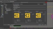
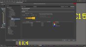
"Stack‑Up to Success" highlights how a carefully planned PCB stack‑up is foundational to preventing warpage, managing impedance, and avoiding manufacturing delays by clearly communicating layer construction, materials, and tolerance requirements to fabricators.

Read More
Embedded thumbnail for Coming Soon: Sawtooth Rounding Support for Length Tuning
New in Altium Designer 25 • Jul 31, 2025
Coming Soon: Sawtooth Rounding Support for Length Tuning

Sawtooth Rounding for Length Tuning improves signal‑path accuracy by applying controlled corner‑rounding to sawtooth geometries during both Interactive Length Tuning and within‑pair matching in the Auto Tuning engine. Discover this capability and additional innovations on our Coming Soon page.

Start Watching
Blog • Jul 30, 2025
IC Components Explained: A Comprehensive Guide to Integrated Circuits

Gain a clear understanding of the fundamental elements within integrated circuits. This guide examines their structure, function, and role in system performance, knowledge that’s vital for anyone involved in sourcing or developing electronic designs.

Read More
Embedded thumbnail for Coming Soon: Z-Axis Clearance Rule
New in Altium Designer 25 • Jul 29, 2025
Coming Soon: Z-Axis Clearance Rule

The Z-Axis Clearance Rule checks the shortest distance between copper features on different layers in a PCB design. It is available in both the Constraint Manager and the legacy PCB Rules Editor. Discover more new features in Altium on our Coming Soon Page.

Start Watching
Blog • Jul 28, 2025
Ensuring Precise Connector Alignment in Multi‑Board Manufacturing

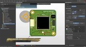
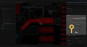
Misaligned connectors can cause major issues in multi-board assemblies. In this article, David Marrakchi shows how Altium’s 3D tools help detect and fix alignment problems early in the design process.

Read More
Embedded thumbnail for Coming Soon: Advanced Polygon Pour Engine
New in Altium Designer 25 • Jul 24, 2025
Coming Soon: Advanced Polygon Pour Engine

Now supports true arcs instead of approximated curves in copper pours. This enhanced engine marks a major advancement in the polygon pour process in Altium Designer, delivering smoother and more accurate copper shapes. Native arc rendering improves visual quality and helps ensure cleaner, more professional PCB designs.

Start Watching
Blog • Jul 23, 2025
Getting Started with the Renesas RA8D1 Evaluation Kit and Edge AI

Dive into the power of Renesas’ RA8D1 MCU using the EK‑RA8D1 evaluation kit. Learn how to train, test, and deploy image‑based detection models seamlessly with Edge Impulse, and kickstart your embedded vision AI projects in minutes.

Read More
Embedded thumbnail for How to Design Rigid-Flex PCB Stackups from Scratch
How-To's • Jul 22, 2025
How to Design Rigid-Flex PCB Stackups from Scratch

Watch this tutorial to learn the fundamentals of Rigid-Flex design. We cover everything from understanding polyimide materials and adhesive layers to building complex, multi-layer Rigid-Flex constructions that are ready for manufacturing.

Start Watching
Blog • Jul 21, 2025
How to Effectively Use Jira for Hardware Development Projects

Originally built for software development, Jira has become a popular tool for agile project management across various industries. Our new article explores how hardware teams can leverage core Jira features and adapt agile principles to suit the unique needs of hardware development.

Read More
Embedded thumbnail for How to Draw Antipads - Complete Tutorial
How-To's • Jul 17, 2025
How to Draw Antipads - Complete Tutorial

Discover how to draw and define antipads in Altium with this complete tutorial. Learn three different methods for creating antipads around vias. From simple design rules to advanced polygon cutouts for both basic and complex PCB designs.

Start Watching
Blog • Jul 16, 2025
Building Supply Chain Resilience: Transforming BOM Management for Modern Electronics

Discover why top electronics companies are replacing spreadsheets with purpose-built BOM management solutions. This whitepaper outlines the risks of outdated methods, offers a readiness checklist, and explores how BOM Portal helps teams cut costs, reduce risk, and speed up development with smarter, data-driven workflows.

Read More
Embedded thumbnail for Do PCB Manufacturers Actually Look at Fabrication Drawings?
How-To's • Jul 15, 2025
Do PCB Manufacturers Actually Look at Fabrication Drawings?

Explore this in-depth tutorial featuring real fabrication drawings, stackup specifications, and drill tables - all created using Altium Designer’s Draftsman tool. Learn essential insights into PCB data management and manufacturing requirements from an industry perspective.

Start Watching
Blog • Jul 14, 2025
Material and Process Considerations That Influence Performance

Material and process choices play a key role in high-performance PCB design. This article highlights how stack-up configuration, substrate selection, and lamination strategy impact signal integrity, reliability, and manufacturability.

Read More
  • Show More
Tag (field_common_tag)
Recovering Copper Losses
Blog • Feb 17, 2022
Recover Conductor Losses By Clearing Your PCB Ground Layer

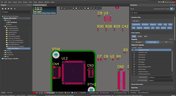
Controlled impedance routing at high frequencies is difficult enough, and it's important to make sure that you stay within your loss budget on long routes or in lossy media. When you have to route a long trace or a long differential pair to a connector or another component, what can you do if you're reaching the end of your loss budget? In this article, we’ll take a look at the skip reference routing method and explain how it can help recover some loss budget in a lossy interconnect.

Read More
Altium 365 SOC 2 Type 1 Certified
Blog • Feb 15, 2022
Announcing SOC 2 Type 1 Certification for Altium 365

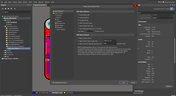
We are pleased to announce that Altium 365 is officially SOC 2 Type 1 certified. System and Organization Controls (SOC) 2 is a widely recognized attestation of security compliance defined by the AICPA and is considered the standard for ensuring data security and operational maturity. A SOC 2 certification provides valuable information for companies to assess the quality of the security provided by a service such as Altium 365.

Read More
Three ways to manage your BOM costs
Blog • Feb 10, 2022
Improving Supply Chain Success with BOM Management

It’s no secret that component shortages have become more frequent this year. Companies will continue to grapple with supply chain challenges into 2022 and beyond. The impact of manufacturing delays can be substantial if a part is not available. Delays occur and sales plans get put on hold. It can also be very expensive and risky to replace parts from multiple sources. Fortunately, many shortages can be avoided by introducing proactive supply chain practices.

Read More
Reliability and failure analysis
Blog • Feb 8, 2022
Overview of PCB/PCBA Reliability and Failure Analysis

Reliability testing and failure analysis of a PCB/PCBA go hand-in-hand; when designs are stressed to the limit, their failure modes need to be determined through thorough inspection and analysis. To get started on this topic, it’s important to understand the qualification aspects that will govern your bare board design and the PCBA. We’ll look at the various dimensions of PCB/PCBA reliability, as well as some of the standard failure analysis techniques used to identify potential design change requirements.

Read More
Plane and Cavity Resonances
Blog • Feb 3, 2022
When Do PCB Power Plane Resonances Occur?

By now, designers should be aware of some important behavior involved in power delivery to components in a PCB, particularly for digital components. All digital components produce and manipulate wideband signals, where the frequency content theoretically extends up to infinite frequency. As such, some radiation may propagate through your PCB, leading to resonant behavior that is not observed on the power rail.

Read More
Selecting a plating material
Blog • Feb 1, 2022
How to Choose PCB Plating for Your Finished Board

Once your board passes through the standard PCB fabrication process, the bare copper in your PCB will be ready for the application of a surface finish. PCB plating is applied to protect any copper in your PCB that would be exposed through the solder mask, whether it’s a pad, via, or other conductive element. In this article, I’ll run over the different PCB plating material options and their advantages in your PCB. 

Read More
What is the PCB Supply Chain?
Blog • Jan 27, 2022
What is the PCB Supply Chain?

The PCB supply chain encompasses multiple components, raw materials, and the PCB itself. PCBs and PCB assemblies are often the most technically complex components that are purchased for electronic assemblies and products. The complexity of modern PCBs leads to several challenges for a supply chain management team that may be significantly different when compared with other commodities the team manages. In this brief guide, we'll look in-depth at the PCB supply chain, and specifically what falls within the purview of a procurement and supply chain management team.

Read More
What is mode conversion
Blog • Jan 25, 2022
A Guide to Mode Conversion, Its Causes, and Solutions

On interconnects, such as board-to-board connections or cascaded transmission line arrangements, you have an important EMC compliance metric that is sometimes overlooked. This is mode conversion, which can be visualized in an S-parameter measurement for differential and common-mode signal transmission. In this article, we’ll look at a short overview of mode conversion in high-speed design with some examples from common differential standards.

Read More
Pad and via sizing
Blog • Jan 20, 2022
PCB Via Size and Pad Size Guidelines

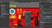
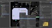
There are some aspects of PCB design and layout that seem deceptively simple, and yet they have a complex answer that is related to many important aspects of manufacturing. One of these design aspects is the match between PCB via size and pad size. Obviously, these two points are related; all vias have a landing pad that supports the via and provides a place to route traces into a via pad. However, there are some important sizing guidelines to follow when the matching pad and via sizes, and this match is an important element of DFM and reliability.

Read More
Differential Microstrip Impedance
Blog • Jan 18, 2022
Differential Microstrip Impedance Calculator

Are you looking for a free tool that you can use to calculate the impedance of differential microstrips? We created a simple tool you can use to calculate differential microstrip impedance for a given geometry and dielectric constant. If you’ve been looking for an accurate differential microstrip impedance calculator, then the calculator below is certainly one of the best free tools you’ll find on the internet before you start using field solvers to determine differential pair impedance.

Read More
PCB DFM Check
Blog • Jan 13, 2022
Getting Through a PCB DFM Check

In this article, we’ll discuss the key design features to implement, and steps to take prior to fabrication that will help prevent some common DFM problems. I’ll also provide examples of where I commonly see these PCB DFM problems in signal integrity circuits.

Read More
Spreading Inductance
Blog • Jan 11, 2022
What is Spreading Inductance?

If you’re working with a high-speed digital component, there are some simple power integrity rules that should be followed. However, there is one quantity that is sometimes ignored when building a PDN impedance simulation: the spreading inductance of your plane pair. Here are some points designers should know about the spreading inductance of a plane pair.

Read More
PCB Design Basics for New Designers
Blog • Jan 6, 2022
PCB Design Basics for New Designers

In this article, I’ll present some design basics that every new designer should follow to help ensure their design process is successful. Some of these points may challenge the conventional view of how circuit boards are constructed, but they are intended to help balance low noise signaling, manufacturability, and ease of solving a layout.

Read More
Selecting Materials for High Voltage PCB Design and Layout
Blog • Jan 4, 2022
Selecting Materials for High Voltage PCB Design and Layout

High voltage PCBs are subject to certain safety and reliability concerns that you won’t find in most other boards. If your fabrication house specializes in high voltage PCBs and keeps materials in stock, they can likely recommend a material set, as well as a standard stackup you might use for certain voltage ranges and frequencies. If you need to choose your own materials, follow the tips below to help you narrow down to the right material set.

Read More
Via tenting in PCB Layout
Blog • Dec 28, 2021
When to Use Tented Vias in Your PCB Layout

There are some guidelines I see many designers implement as a standard practice, often without thinking about it. Some of these practices are misunderstood or implemented without best practices. Others are implemented without thinking about the potential problems. One of these is the use of tented vias, which is sometimes implemented in a PCB layout by default. Is this always the right practice?

Read More
Capacitive load termination
Blog • Dec 23, 2021
How to Impedance Match and Terminate Capacitive Loads

The idea of a purely capacitive load is something of a fallacy. Yes, capacitors exist, but all capacitors are non-ideal, and it is this deviation from a theoretical capacitance that determines how to impedance match a load that exhibits capacitive behavior. Let’s take a look at this important aspect of interconnect design and see what it really means to terminate a capacitive load.

Read More
  • Show More
Tag (field_common_tag)
Embedded thumbnail for Searching for Errors
• Jun 16, 2020
Searching for Errors

We’ve looked at how to set up the Design Rule Checker to help us analyze our PCB design errors. Now it’s time to resolve these errors and prep our design to start generating output files.

Start Watching
Embedded thumbnail for Performing Board DRC
• Jun 16, 2020
Performing Board DRC

Design rules are crucial to a PCB’s overall design and performance. It’s just as important to adhere to these rules and ensure that we didn’t overlook any unconnected nets or short circuits. This is why we need to run a Design Rule check.

Start Watching
Embedded thumbnail for Placing a Custom 3D Body in 3D View
• Jun 16, 2020
Placing a Custom 3D Body in 3D View

With the help of the 3D view, it is possible to view a PCB design from all sides, to check on component placement, silkscreen alignment, and many other visual aspects.

Start Watching
Embedded thumbnail for Silkscreen Placement
• Jun 16, 2020
Silkscreen Placement

The silkscreen layer is the layer on which we print any visual text or symbols on our PCB. With the help of this silkscreen layer, we can print our component designators, pin placement, and more.

Start Watching
Embedded thumbnail for Working with Polygon Pours
• Jun 16, 2020
Working with Polygon Pours

When working with common signals, the current levels are usually quite minimal, but when working with power nets it’s not uncommon to see current levels of a few amps. One of the reasons to use polygons is to maintain the quality and reliability of the power supply system.

Start Watching
Embedded thumbnail for Routing Post Processes
• Jun 16, 2020
Routing Post Processes

Depending on how you routed your board, it may be a time-consuming process to fix these manually. So we’ll dive into Route Glossing a little more, along with an automated way to retrace pre-existing routes.

Start Watching
Embedded thumbnail for PCB Layout Cleanup
• Jun 16, 2020
PCB Layout Cleanup

After the board has been routed, it’s almost certain that you’ll need to either move, delete, or adjust some traces. We’ll be looking at a few basic methods to easily modify and remove traces in our design.

Start Watching
Embedded thumbnail for Differential Pair Routing
• Jun 16, 2020
Differential Pair Routing

Routing Differential Pairs is similar to routing single traces, but there are additional rules and guidelines to follow that will help you avoid signal integrity problems.

Start Watching
Embedded thumbnail for Introduction to Routing
• Jun 16, 2020
Introduction to Routing

We’ve looked at different routing behaviors and options that we can change to make routing much easier. So we’re going to dive into the basics of routing and how these settings and routing modes can be applied.

Start Watching
Embedded thumbnail for Defining the Layer Stackup
• Jun 10, 2020
Defining the Layer Stackup

The PCB is designed and formed as a stack of layers and the definition of the PCB layer stack is a critical element of successful printed circuit board design. In Altium Designer, the Layer Stack Manager is used to develop the printed circuit board internal design including layer-pairing, careful via design, any back drilling requirements, rigid/flex requirements, copper balancing, layer stack symmetry, and material compliance. This video guides you through creation of a layer stackup, adding the necessary layers, as well as adding an impedance profile.

Start Watching
Embedded thumbnail for Searching for Errors in Schematic
• May 20, 2020
Searching for Errors in Schematic

Searching for Errors: Errors and mistakes happen to everyone - from beginners to professionals. So we always preach how it is paramount for your design to be validated before pushing it to the PCB. But luckily it’s pretty easy to find and analyze any errors using Altium Designer. We’ll take a look at how to find and analyze errors in your schematic.

Start Watching
Embedded thumbnail for Creating Net Classes
• Jun 2, 2020
Creating Net Classes

A Net Class is a collection of nets that can be used for creating a targeted design rule. So for example, you may want all power and ground nets to have a minimum track width to handle a specific current rating. So we’ll show you how to assign these nets to a NetClass. 

Start Watching
Embedded thumbnail for Configuring Design Rules - Part 2
• May 14, 2020
Configuring Design Rules - Part 2

Altium Designer uses the concept of Design Rules to define the requirements of a design. These rules collectively form an instruction set for the PCB Editor to follow. They cover every aspect of the design - from routing widths, clearances, plane connection styles and so on. With a well-defined set of design rules, you can successfully complete board designs with varying and often stringent design requirements.

Start Watching
Embedded thumbnail for Routing Modes and Setup
• May 12, 2020
Routing Modes and Setup

Most of you know that routing can be a time consuming process, but it doesn’t have to be a daunting task if you have the right tools. So we’ll be looking at what options and settings can help us perfect the art of routing.

Start Watching
Embedded thumbnail for PCB Component Placement
• May 12, 2020
PCB Component Placement

Component placement in the PCB is an important stage of the design process as it sets the precedent for efficient and clean routing. We’ll be diving into different component placement methods along with some tips and tricks that you can use to make this an easy process. 

Start Watching
Embedded thumbnail for Configuring the Basic Rules
• May 12, 2020
Configuring the Basic Rules

Altium Designer uses the concept of Design Rules to define the requirements of a design. These rules collectively form an instruction set for the PCB Editor to follow. They cover every aspect of the design - from routing widths, clearances, plane connection styles and so on. With a well-defined set of design rules, you can successfully complete board designs with varying and often stringent design requirements.

Start Watching
  • Show More
Tag (field_common_tag)
ADv25
On-Demand Webinar • Oct 24, 2024
Modernizing Engineering Workflows: Altium Designer 25 and the Future of Concurrent Design
Struggling with team misalignment and design errors? Join our exciting webinar to discover the groundbreaking advancements in Altium Designer 25!
Watch Now
KiCad Webinar
On-Demand Webinar • Oct 16, 2024
Taking the Next Step: Growing Beyond KiCad with Altium
Join our upcoming webinar to discover how Altium Designer can transition your KiCad projects without any data loss
Watch Now
Synchronize to Optimize Jira Integration
On-Demand Webinar • Oct 7, 2024
Synchronize to Optimize: Enhancing Efficiency with Jira Integration for Altium 365
Tired of juggling multiple tools for project management? Watch the webinar and see how Jira Integration for Altium 365 can optimize your workflows.
Watch Now
Wire bonding
On-Demand Webinar • Sep 29, 2024
Unlock New Design Possibilities with Wire Bonding
Explore how wire bonding can enhance your designs, provide size reduction, improve power management, and increase mechanical reliability.
Watch Now
routing
On-Demand Webinar • Sep 29, 2024
Advanced Routing Features & Techniques
To help you get the most out of your experience with Altium Designer, join our webinar this month and learn advanced routing techniques.
Watch Now
signal analyzer
On-Demand Webinar • Sep 25, 2024
Signal Integrity Made Simple
Discover how to easily detect and resolve high-speed signal integrity challenges without the need for extensive expertise.
Watch Now
competitive-displacement-webinar-3
On-Demand Webinar • Sep 20, 2024
Mastering Design Complexity: How Altium Designer Outperforms Cadence in Solving Workflow and Engineering Challenges - Part 2
Join our webinar to learn how to enhance efficiency, foster better collaboration, and accelerate your time-to-market with Altium unified solutions.
Watch Now
Breaking Down Silos Webinar
On-Demand Webinar • Sep 16, 2024
Breaking Down Data Silos: A Practical Comparison of Altium and Cadence in Cross-Functional PCB Design
Join us for a webinar that addresses the critical challenges of maintaining design data continuity across various design functions.
Watch Now
Draftsman
On-Demand Webinar • Sep 10, 2024
Mastering Design Complexity: How Altium Designer Outperforms Cadence in Solving Workflow and Engineering Challenges
Join our upcoming webinar to discover why engineers consistently choose Altium Designer as the standard in PCB design.
Watch Now
SPICE
On-Demand Webinar • Sep 3, 2024
Mastering SPICE Simulation in Altium Designer
Discover how the SPICE engine in Altium Designer can help you easily verify that your finished project functions as intended.
Watch Now
Output job
On-Demand Webinar • Aug 24, 2024
Beyond PCB Design with Altium Designer
In this webinar we'll dive into the essential aspects that go beyond the schematic and layout.
Watch Now
PCB
On-Demand Webinar • Aug 23, 2024
Elevate Your Design Skills: Tips & Tricks for Success
Discover practical insights and efficient methods that can enhance your PCB design capabilities.
Watch Now
Cyber Security Webinar Cover
On-Demand Webinar • Aug 6, 2024
The Anatomy of IT Compliance in Electronics Development: Altium 365 & AWS GovCloud
Are you an IT or security professional looking for a secure electronics design collaboration platform that could also support your ITAR and EAR compliance efforts? If so, watch this webinar to bring together the expertise of Altium 365 and AWS!
Watch Now
Design reuse
On-Demand Webinar • Aug 1, 2024
How to Speed-up Product Development with Reusable Circuitry
In this webinar you'll learn more about the benefits of the design reuse blocks approach as well as the Design Reuse panel.
Watch Now
Harness design
On-Demand Webinar • Jul 19, 2024
Stay Ahead of the Curve: A Half-Year Review of Altium Designer Improvements
Join our exciting webinar to discover the groundbreaking advancements in Altium Designer!
Watch Now
Lenght Tuning
On-Demand Webinar • Jun 26, 2024
Achieve Precision and Speed with Altium Designer 24's Innovative Routing Features
Speed up your routing process and achieve better results for even your most demanding designs.
Watch Now
  • Show More
Tag (field_common_tag)
Loading
Loading...
Share link
Share with
Search by Update
Version
Update
25 26 24 23 22
25.0 25.1 25.2 25.3 25.4 25.5 25.6 25.7 25.8 25.9
26.1 26.2
24.10 24.9 24.8 24.7 24.6 24.5 24.4 24.3 24.2 24.1 24.0
23.11 23.10 23.9 23.8 23.7 23.6 23.5 23.4 23.3 23.2 23.1 23.0
22.11 22.10 22.9 22.8 22.7 22.6 22.5 22.4 22.3