
Main navigation

  • Home
  • Discover
  • Learning Center
  • What’s New

Second main navigation

  • Altium Community
  • Support
  • Documentation
×

Results

  • Updates
  • Blog 570
  • Video 539
  • Webinar 86
  • Playlist 53
Filters:
Tag (field_common_tag)
Embedded thumbnail for PCB Library Management: One Library or Many?
How-To's • Aug 5, 2025
PCB Library Management: One Library or Many?

This detailed guide walks you through the pros and cons of each approach and offers proven strategies for managing component data, whether you're an independent designer or overseeing libraries for an entire organization.

Start Watching
Blog • Aug 4, 2025
Stack-Up to Success: Avoid the Pitfalls

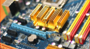
"Stack‑Up to Success" highlights how a carefully planned PCB stack‑up is foundational to preventing warpage, managing impedance, and avoiding manufacturing delays by clearly communicating layer construction, materials, and tolerance requirements to fabricators.

Read More
Embedded thumbnail for Coming Soon: Sawtooth Rounding Support for Length Tuning
New in Altium Designer 25 • Jul 31, 2025
Coming Soon: Sawtooth Rounding Support for Length Tuning

Sawtooth Rounding for Length Tuning improves signal‑path accuracy by applying controlled corner‑rounding to sawtooth geometries during both Interactive Length Tuning and within‑pair matching in the Auto Tuning engine. Discover this capability and additional innovations on our Coming Soon page.

Start Watching
Blog • Jul 30, 2025
IC Components Explained: A Comprehensive Guide to Integrated Circuits

Gain a clear understanding of the fundamental elements within integrated circuits. This guide examines their structure, function, and role in system performance, knowledge that’s vital for anyone involved in sourcing or developing electronic designs.

Read More
Embedded thumbnail for Coming Soon: Z-Axis Clearance Rule
New in Altium Designer 25 • Jul 29, 2025
Coming Soon: Z-Axis Clearance Rule

The Z-Axis Clearance Rule checks the shortest distance between copper features on different layers in a PCB design. It is available in both the Constraint Manager and the legacy PCB Rules Editor. Discover more new features in Altium on our Coming Soon Page.

Start Watching
Blog • Jul 28, 2025
Ensuring Precise Connector Alignment in Multi‑Board Manufacturing

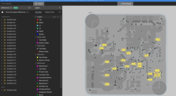
Misaligned connectors can cause major issues in multi-board assemblies. In this article, David Marrakchi shows how Altium’s 3D tools help detect and fix alignment problems early in the design process.

Read More
Embedded thumbnail for Coming Soon: Advanced Polygon Pour Engine
New in Altium Designer 25 • Jul 24, 2025
Coming Soon: Advanced Polygon Pour Engine

Now supports true arcs instead of approximated curves in copper pours. This enhanced engine marks a major advancement in the polygon pour process in Altium Designer, delivering smoother and more accurate copper shapes. Native arc rendering improves visual quality and helps ensure cleaner, more professional PCB designs.

Start Watching
Blog • Jul 23, 2025
Getting Started with the Renesas RA8D1 Evaluation Kit and Edge AI

Dive into the power of Renesas’ RA8D1 MCU using the EK‑RA8D1 evaluation kit. Learn how to train, test, and deploy image‑based detection models seamlessly with Edge Impulse, and kickstart your embedded vision AI projects in minutes.

Read More
Embedded thumbnail for How to Design Rigid-Flex PCB Stackups from Scratch
How-To's • Jul 22, 2025
How to Design Rigid-Flex PCB Stackups from Scratch

Watch this tutorial to learn the fundamentals of Rigid-Flex design. We cover everything from understanding polyimide materials and adhesive layers to building complex, multi-layer Rigid-Flex constructions that are ready for manufacturing.

Start Watching
Blog • Jul 21, 2025
How to Effectively Use Jira for Hardware Development Projects

Originally built for software development, Jira has become a popular tool for agile project management across various industries. Our new article explores how hardware teams can leverage core Jira features and adapt agile principles to suit the unique needs of hardware development.

Read More
Embedded thumbnail for How to Draw Antipads - Complete Tutorial
How-To's • Jul 17, 2025
How to Draw Antipads - Complete Tutorial

Discover how to draw and define antipads in Altium with this complete tutorial. Learn three different methods for creating antipads around vias. From simple design rules to advanced polygon cutouts for both basic and complex PCB designs.

Start Watching
Blog • Jul 16, 2025
Building Supply Chain Resilience: Transforming BOM Management for Modern Electronics

Discover why top electronics companies are replacing spreadsheets with purpose-built BOM management solutions. This whitepaper outlines the risks of outdated methods, offers a readiness checklist, and explores how BOM Portal helps teams cut costs, reduce risk, and speed up development with smarter, data-driven workflows.

Read More
Embedded thumbnail for Do PCB Manufacturers Actually Look at Fabrication Drawings?
How-To's • Jul 15, 2025
Do PCB Manufacturers Actually Look at Fabrication Drawings?

Explore this in-depth tutorial featuring real fabrication drawings, stackup specifications, and drill tables - all created using Altium Designer’s Draftsman tool. Learn essential insights into PCB data management and manufacturing requirements from an industry perspective.

Start Watching
Blog • Jul 14, 2025
Material and Process Considerations That Influence Performance

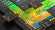
Material and process choices play a key role in high-performance PCB design. This article highlights how stack-up configuration, substrate selection, and lamination strategy impact signal integrity, reliability, and manufacturability.

Read More
Embedded thumbnail for Compensating Transmission Line Losses in a PCB Calculator
How-To's • Jul 10, 2025
Compensating Transmission Line Losses in a PCB Calculator

This tutorial uncovers the key difference between ideal, lossless impedance calculations and real-world signal behavior giving you practical techniques to design controlled impedance PCBs that deliver reliable performance.

Start Watching
Blog • Jul 9, 2025
How to Make Your PCB Layout AOI and X-Ray Friendly

Designing for inspection is key to reliable manufacturing. This article covers practical PCB layout tips to optimize your board for AOI and X-ray inspection helping you reduce defects, false positives, and production delays.

Read More
  • Show More
Tag (field_common_tag)
Blog • Apr 25, 2023
Mechanical and Electrical Design Come Together With Altium’s MCAD CoDesigner

Electronics designers working in small design houses or in large enterprises often encounter a common set of challenges when interfacing with mechanical designers. Continue reading to learn how you can best interface with your mechanical designer to get your projects out the door fast!

Read More
DRC
Blog • Apr 13, 2023
DRC/ERC in WebViewer
Altium 365 Web Viewer now displays reports on Design Rule Checking (DRC) and Electrical Rule Checking (ERC) for your project, which makes reviewing easier as you can check for rule errors or violations without opening the design in Altium Designer.
Read More
Blog • Apr 4, 2023
Ebook: Routing High-Density Interconnects with Reliable Microvias

HDI PCBs take a particular approach to routing interconnects through multiple layers to ensure reliability during fabrication, assembly, and operation. The critical structure that enables this is microvias, which are prone to failure if not designed properly. In this e-book, readers will receive an initial look at the reasons microvia reliability has come into the spotlight and why HDI PCB designers put reliability first when routing through microvias.

Read More
Altium 365 Personal now supports ODB++ manufacturing data storage and management in your personal workspace.
Blog • Apr 3, 2023
ODB++ in Altium 365 Personal Space
Altium 365 Personal now supports ODB++ manufacturing data storage and management in your personal workspace.
Read More
GovCloud
Blog • Mar 29, 2023
Altium 365 GovCloud

Introducing Altium 365 GovCloud - a dedicated region of the Altium 365 cloud platform designed for regulated companies and organizations handling sensitive data. 

Read More
https://www.altium.com/altium-365/whats-new#new-default-preferences-for-altium-365-web-viewer
Blog • Mar 27, 2023
New Default Preferences for Altium 365 Web Viewer
Our primary objective is maintaining consistency in the project view between Altium Designer and Altium 365 Web Viewer. In the past, the default Altium Designer preferences used in the Altium 365 Web Viewer created discrepancies when non-default preferences were employed, leading to incorrect design displays during design reviews.
Read More
MCAD CoDesigner 3.4.0
Blog • Mar 24, 2023
MCAD CoDesigner 3.4.0

The newest release of MCAD CoDesigner 3.4.0 is finally here, and it comes packed with amazing features and improvements that will change how you work.

Read More
Design Review
Blog • Mar 22, 2023
Design Review Challenge Winners

We're proud to announce the PCB Design Review Challenge winners by Altium. ? Thank you to all the participants of this competition, and congratulations to the lucky winners!

Read More
Blog • Mar 21, 2023
IPC-2221 Calculator for PCB Trace Current and Heating

Aside from impedance and annular ring calculations, one of the other major formulas specified in the IPC 2221 standard relates temperature rise, trace width, and trace current. THere is also the IPC-2152 standard, both include this guidance on designing for thermal reliability, but which standard should we use?

Read More
Blog • Mar 16, 2023
Multiple PCBs and Panels Support in Altium 365 Web Viewer

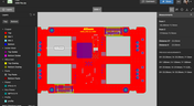
We are delighted to announce the release of a new feature that allows you to view multiple PCB documents in your project, including panel PCBs. This feature streamlines your design process, enabling you to access and collaborate on your entire PCB design in one central location.

Read More
Blog • Mar 14, 2023
PCB Compare in Altium 365 Web Viewer

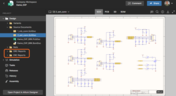
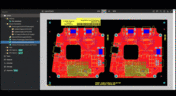
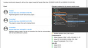
Altium 365 has enhanced its compare capabilities by adding PCB Compare operations between different commits/releases of managed projects. This latest feature, which complements Altium 365's existing compare capabilities for schematic, BOM, and Gerber files, provides users with comprehensive tools for reviewing and analyzing design changes.

Read More
Blog • Mar 2, 2023
Stripline Impedance Calculator

Striplines provide some advantages over microstrips as they take advantage of natural shielding and coupling from nearby ground plane layers. Although they tend to experience higher losses due to total confinement in the dielectric, they can be thinner due to the high dielectric constant used in internal layers of a PCB. Use our free impedence calculator to help you determine the correct width needed to hit a target impedance.

Read More
Blog • Mar 1, 2023
Project History Export

Altium Designer now offers the added capability to share project history reports with third-party entities in PDF format, while enabling users to save them as release artifacts for backup and internal auditing purposes.

Read More
Blog • Feb 23, 2023
Which Types of Opto-Isolators Are Right For Your Signal?

An optoisolator is a cool electronic device that can be used to pass information between a diode without passing an electrical current. There are many great applications for these, but do you know which one is right for you?

Read More
Blog • Feb 22, 2023
Properties panel document options in SCH editors

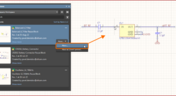
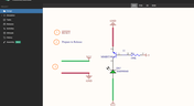
The Properties panel provides access to the properties of documents and objects. The contents of the panel change depending on the active document or the selected object. This blog will quickly go over some of need to know options around the properties panel in the schematic document.

Read More
Blog • Feb 17, 2023
Part Choices Revision Control

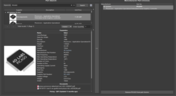
The revision-controlled part choice enforces special control over parts. Each set of modifications is captured in a snapshot of the item record called a revision. Each revision represents the state of that item at a particular instance in time. When a new revision is created, the previous revision of the item is permanently locked and cannot be changed.

Read More
  • Show More
Tag (field_common_tag)
Embedded thumbnail for Creating a PCB Footprint Courtyard
How to create a PCB Footprint • Jul 27, 2022
Creating a PCB Footprint Courtyard

The courtyard is an essential piece when you want to create a PCB Footprint in Altium Designer. We’ll talk about what a courtyard is, how to create a courtyard, and how to format a courtyard correctly for your PCB footprint.

Start Watching
Embedded thumbnail for How to Edit Existing Tracks in Altium Designer
How-To's • Jul 25, 2022
How to Edit Existing Tracks in Altium Designer

This new design rule flags a violation when the creepage distance across non-conductive surface and edge regions of the board, between the targeted signals, is equal to or less than the specified Creepage distance.

Start Watching
Embedded thumbnail for Creating a PCB Footprint Silkscreen Overlay
How to create a PCB Footprint • Jul 22, 2022
Creating a PCB Footprint Silkscreen Overlay

When creating a PCB footprint in Altium Designer creating a silkscreen overlay is an important requirement. We’ll go over the standards for creating a silkscreen overlay for a footprint and the steps to creating one, such as constructing lines and measuring distance of objects and primitives.

Start Watching
Embedded thumbnail for Adding Designators for Assembly Drawings
How-To's • Jul 18, 2022
Adding Designators for Assembly Drawings

Designators for assembly drawings are added on the assembly layer. This video shows how to add the designators.

Start Watching
Embedded thumbnail for Stackup Material Library
How to work with Layer Stack Manager • Jul 15, 2022
Stackup Material Library

In this video we will learn more about the Altium designers Layer Stack Mangers built-in materials library, and how to add new material and use it in our board stack. We will also look at how we can save the user materials to an xml format.

Start Watching
Embedded thumbnail for Placing Footprint Pads
How to create a PCB Footprint • Jul 13, 2022
Placing Footprint Pads

Every footprints needs proper pad placement to ensure trace connectivity. Placing pads is the first step towards footprint creation.

Start Watching
Embedded thumbnail for Setting the Transparency for Layers and Primitives
How-To's • Jul 11, 2022
Setting the Transparency for Layers and Primitives

Customize your workspace by setting the transparency of layers and primitives in the PCB.

Start Watching
Embedded thumbnail for Create New Via Types Using the Layer Stack Manager
How to work with Layer Stack Manager • Jul 8, 2022
Create New Via Types Using the Layer Stack Manager

In this video, we will learn how to create new via types using the Layer Stack Manager, and how to create new Routing Via design rules using the PCB Rules and Constraints Editor. We will also explore how to use the different types of Via during interactive routing.

Start Watching
Embedded thumbnail for How to Create a Copper Board Report
How-To's • Jul 4, 2022
How to Create a Copper Board Report

This video will show how to create a copper board report in your PCB which can be useful for copper balance in DFM process

Start Watching
Embedded thumbnail for Stackup Creation and editing
How to work with Layer Stack Manager • Jul 1, 2022
Stackup Creation and editing

This video shows how to view and edit the PCB Layer Stack, select materials and add new layers

Start Watching
Embedded thumbnail for Configuring Your PCB Library
How to create a PCB Footprint • Jun 29, 2022
Configuring Your PCB Library

It is important to have accurate footprints to manufacture your PCB. Learn how to configure your PCB library to facilitate footprint creation.

Start Watching
Embedded thumbnail for How to Validate Links Between Components and Footprints
How-To's • Jun 27, 2022
How to Validate Links Between Components and Footprints

Before importing or updating data from the circuit to the board, you must first verify that all components of the circuit are associated with Footprint. Watch this video to learn how to validate the links between your schematic components and footprints.

Start Watching
Embedded thumbnail for How to use Copy Room Format
How to work with Rooms • Jun 24, 2022
How to use Copy Room Format

Rooms allow you to use rules on specific areas of your design. This helps immensely with properly defining trace widths and hole sizes for specific components. We’ll show you how easy it is to assign rules to specific rooms in the PCB.

Start Watching
Embedded thumbnail for How To Do Versioning And Releases by Robert Feranec and Michal Faruga
Discovering Altium 365 • Jun 20, 2022
How To Do Versioning And Releases by Robert Feranec and Michal Faruga

Meet Robert Feranec in an educational video on version control, project history, comments, comparison and other features in Altium Designer 

Start Watching
Embedded thumbnail for Using Rooms in Rules
How to work with Rooms • Jun 17, 2022
Using Rooms in Rules

Rooms allow you to use rules on specific areas of your design. This helps immensely with properly defining trace widths and hole sizes for specific components. We’ll show you how easy it is to assign rules to specific rooms in the PCB.

Start Watching
Embedded thumbnail for Creating a Schematic Symbol: Dealing with Power Pins
How to create a Schematic Symbol • Jun 15, 2022
Creating a Schematic Symbol: Dealing with Power Pins

Multiple schematic symbols often require the use of multiple power and ground pins. We’ll show you the difference between hidden and visible power pins, and the various methods you can use to use them in your design however it works best for you.

Start Watching
  • Show More
Tag (field_common_tag)
ADv25
On-Demand Webinar • Oct 24, 2024
Modernizing Engineering Workflows: Altium Designer 25 and the Future of Concurrent Design
Struggling with team misalignment and design errors? Join our exciting webinar to discover the groundbreaking advancements in Altium Designer 25!
Watch Now
KiCad Webinar
On-Demand Webinar • Oct 16, 2024
Taking the Next Step: Growing Beyond KiCad with Altium
Join our upcoming webinar to discover how Altium Designer can transition your KiCad projects without any data loss
Watch Now
Synchronize to Optimize Jira Integration
On-Demand Webinar • Oct 7, 2024
Synchronize to Optimize: Enhancing Efficiency with Jira Integration for Altium 365
Tired of juggling multiple tools for project management? Watch the webinar and see how Jira Integration for Altium 365 can optimize your workflows.
Watch Now
Wire bonding
On-Demand Webinar • Sep 29, 2024
Unlock New Design Possibilities with Wire Bonding
Explore how wire bonding can enhance your designs, provide size reduction, improve power management, and increase mechanical reliability.
Watch Now
routing
On-Demand Webinar • Sep 29, 2024
Advanced Routing Features & Techniques
To help you get the most out of your experience with Altium Designer, join our webinar this month and learn advanced routing techniques.
Watch Now
signal analyzer
On-Demand Webinar • Sep 25, 2024
Signal Integrity Made Simple
Discover how to easily detect and resolve high-speed signal integrity challenges without the need for extensive expertise.
Watch Now
competitive-displacement-webinar-3
On-Demand Webinar • Sep 20, 2024
Mastering Design Complexity: How Altium Designer Outperforms Cadence in Solving Workflow and Engineering Challenges - Part 2
Join our webinar to learn how to enhance efficiency, foster better collaboration, and accelerate your time-to-market with Altium unified solutions.
Watch Now
Breaking Down Silos Webinar
On-Demand Webinar • Sep 16, 2024
Breaking Down Data Silos: A Practical Comparison of Altium and Cadence in Cross-Functional PCB Design
Join us for a webinar that addresses the critical challenges of maintaining design data continuity across various design functions.
Watch Now
Draftsman
On-Demand Webinar • Sep 10, 2024
Mastering Design Complexity: How Altium Designer Outperforms Cadence in Solving Workflow and Engineering Challenges
Join our upcoming webinar to discover why engineers consistently choose Altium Designer as the standard in PCB design.
Watch Now
SPICE
On-Demand Webinar • Sep 3, 2024
Mastering SPICE Simulation in Altium Designer
Discover how the SPICE engine in Altium Designer can help you easily verify that your finished project functions as intended.
Watch Now
Output job
On-Demand Webinar • Aug 24, 2024
Beyond PCB Design with Altium Designer
In this webinar we'll dive into the essential aspects that go beyond the schematic and layout.
Watch Now
PCB
On-Demand Webinar • Aug 23, 2024
Elevate Your Design Skills: Tips & Tricks for Success
Discover practical insights and efficient methods that can enhance your PCB design capabilities.
Watch Now
Cyber Security Webinar Cover
On-Demand Webinar • Aug 6, 2024
The Anatomy of IT Compliance in Electronics Development: Altium 365 & AWS GovCloud
Are you an IT or security professional looking for a secure electronics design collaboration platform that could also support your ITAR and EAR compliance efforts? If so, watch this webinar to bring together the expertise of Altium 365 and AWS!
Watch Now
Design reuse
On-Demand Webinar • Aug 1, 2024
How to Speed-up Product Development with Reusable Circuitry
In this webinar you'll learn more about the benefits of the design reuse blocks approach as well as the Design Reuse panel.
Watch Now
Harness design
On-Demand Webinar • Jul 19, 2024
Stay Ahead of the Curve: A Half-Year Review of Altium Designer Improvements
Join our exciting webinar to discover the groundbreaking advancements in Altium Designer!
Watch Now
Lenght Tuning
On-Demand Webinar • Jun 26, 2024
Achieve Precision and Speed with Altium Designer 24's Innovative Routing Features
Speed up your routing process and achieve better results for even your most demanding designs.
Watch Now
  • Show More
Tag (field_common_tag)
Loading
Loading...
Share link
Share with
Search by Update
Version
Update
25 26 24 23 22
25.0 25.1 25.2 25.3 25.4 25.5 25.6 25.7 25.8 25.9
26.1 26.2
24.10 24.9 24.8 24.7 24.6 24.5 24.4 24.3 24.2 24.1 24.0
23.11 23.10 23.9 23.8 23.7 23.6 23.5 23.4 23.3 23.2 23.1 23.0
22.11 22.10 22.9 22.8 22.7 22.6 22.5 22.4 22.3