
Main navigation

  • Home
  • Discover
  • Learning Center
  • What’s New

Second main navigation

  • Altium Community
  • Support
  • Documentation
×

Results

  • Updates
  • Blog 570
  • Video 539
  • Webinar 86
  • Playlist 53
Filters:
Tag (field_common_tag)
Blog • Oct 2, 2025
Most Common Causes of PCB Assembly Rework and Scrap

Many PCB assemblies fail not because of exotic faults, but due to basic issues like incorrect BOM entries or footprint mismatches that force rework or scrap. This article dives into the most common causes and how to prevent costly defects in your design-to-manufacturing process.

Read More
Embedded thumbnail for Mechanically Drilled Blind & Buried Vias: PCB Design Rules Explained
How-To's • Oct 1, 2025
Mechanically Drilled Blind & Buried Vias: PCB Design Rules Explained

Discover the essential design rules and manufacturing processes for mechanically drilled blind and buried vias in PCB layouts in this comprehensive tutorial. We cover the stack drill-and-plate fabrication process, aspect ratio limitations, sub-lamination design, and copper weight considerations. You’ll also learn how these vias differ from HDI microvias and gain a clear understanding of the critical design constraints needed for successful PCB manufacturing.

Start Watching
Blog • Sep 30, 2025
Behind the Scenes with AI Embedded Development

Forget one-shot AI hacks Ari Mahpour shows the thoughtful, sustainable way to integrate AI into embedded firmware development. Learn the core principles (planning gate, HAL abstraction, observability, timeout design) that can help you push your efficiency 5-10 times in real hardware projects.

Read More
Embedded thumbnail for Altium Training - Design Environment: Navigation with Schematic Workspace
Altium Training • Sep 29, 2025
Altium Training - Design Environment: Navigation with Schematic Workspace

Discover the most important navigation techniques for the schematic workspace using both mouse and keyboard controls. In this tutorial video, you’ll learn how to use the View menu commands for document fitting, area zooming, and object selection, along with advanced navigation shortcuts. Master mouse-based panning and zooming, explore Ctrl key combinations, and practice arrow key movements - all designed to simplify your workflow in the PCB design process.

Start Watching
Blog • Sep 25, 2025
We're heading to PCB West 2025!

Join Altium at PCB West 2025 in Santa Clara, CA, on October 1! Stop by Booth 300 for the official launch of the new Altium platform, built on the foundation of Altium Designer and Altium 365. Be sure to check out our live demos of Altium Develop and Altium Agile.

Read More
Blog • Sep 24, 2025
Peak Electrical Performance in Multi-Board Designs With Advanced Simulation and Compliance Tools

Moving from single-board to multi-board systems is a leap in complexity. You must manage not just routing, but power, signal integrity, mechanical fit, and regulatory requirements across boards. In this article, you’ll discover how Altium’s advanced simulation and compliance tools help engineering teams overcome these challenges and deliver reliable multi-board solutions.

Read More
Embedded thumbnail for Altium Training - Design Environment: The Altium Environment
How-To's • Sep 23, 2025
Altium Training - Design Environment: The Altium Environment

Get familiar with the core workspace layout and navigation methods. In this video, you’ll see how to open schematic and PCB documents, work within the unified design environment, and move between multiple open files using document tabs and keyboard shortcuts.

Start Watching
Blog • Sep 22, 2025
How to Catch Enclosure and Connector Misalignment Before the First Prototype

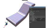
As electronics continue to miniaturize and functionality increases, even minor misalignments between enclosures and connectors can derail a project. This article explores how early integration of ECAD and MCAD workflows helps detect and eliminate those costly issues before the first prototype is built.

Read More
Embedded thumbnail for Altium Training - Design Environment: Opening a Project from a Local Drive
Altium Training • Sep 18, 2025
Altium Training - Design Environment: Opening a Project from a Local Drive

Get your PCB design workflow off to a smooth start. This Altium tutorial walks you through opening projects from your local directory - a core skill that keeps your process efficient and organized from day one.

Start Watching
Blog • Sep 17, 2025
Executive Insights Into Electronic Product Development Gaps You Need To Close

Electronics hardware development is falling behind broader product development disciplines due to fragmented workflows, poor collaboration, and limited compliance visibility. This gap introduces risk, delays, and missed opportunities but executives see real business value in modernizing electronics development through better integration, traceability, and lifecycle visibility.

Read More
Embedded thumbnail for Altium Essentials: Design Environment
Altium Training • Sep 16, 2025
Altium Essentials: Design Environment

Take control of your PCB design workflow with Altium Essentials: Design Environment. This tutorial module guides you through the fundamentals of workspace management, from handling panels and documents to mastering menus, context commands, and time-saving shortcuts.

Start Watching
Blog • Sep 15, 2025
Sourcing For High-Mix Low-Volume Electronics Manufacturing

High-mix, low-volume (HMLV) electronics manufacturing requires agile sourcing strategies to handle shifting BOMs, erratic lead times, and component volatility. All while controlling costs and ensuring compliance. Cloud-based tools like Altium provide real-time component visibility, BOM collaboration, and supplier integrations to help navigate HMLV complexities.

Read More
Embedded thumbnail for What Makes a Great PCB Design Review Submission?
How-To's • Sep 11, 2025
What Makes a Great PCB Design Review Submission?

Turn your PCB designs into professional-grade submissions. At Altium, we reveal the key practices that transform schematics, layouts, and documentation into review-ready work that stands out. Watch our brand-new tutorial and take your PCB design process to the next level.

Start Watching
Blog • Sep 10, 2025
How to Solve Fit, Form, and Function Challenges in Robotics with ECAD-MCAD Collaboration

As robotics systems become increasingly miniaturized and intricate, ensuring perfect fit, form, and function across electrical and mechanical domains is critical to avoid design setbacks. Real-time ECAD-MCAD integration with two-way sync empowers teams to streamline workflows, reduce PCB rework, and deliver more reliable designs faster.

Read More
Embedded thumbnail for Altium Training - Workspace Folder Structure: Opening the Explorer Panel
Altium Training • Sep 9, 2025
Altium Training - Workspace Folder Structure: Opening the Explorer Panel

Discover the key ways to access the Explorer panel in Altium Designer with this step-by-step tutorial. The video walks you through four different methods, giving you the freedom to choose the approach that best fits your workflow.

Start Watching
Blog • Sep 8, 2025
One Vision, Three Powerful Solutions: Introducing Altium Discover, Altium Develop, and Altium Agile

We are excited to announce the launch of three new platform-based solutions that will transform the way electronic products are designed, built, and delivered: Altium Discover, Altium Develop, and Altium Agile. These solutions are designed to simplify processes, accelerate innovation, and make collaboration seamless across the entire electronics lifecycle. Together, they realize the purpose of Altium and Renesas: To Make Our Lives Easier.

Read More
  • Show More
Tag (field_common_tag)
Blog • Jan 17, 2025
Overview of the Gerber X3 File Format

Want to learn how the Gerber X3 file format simplifies data exchange by unifying assembly and fabrication details in a single file? This article explores the format and its role in streamlining PCB manufacturing.

Read More
Blog • Jan 15, 2025
Save Time and Prevent Errors in Cable Harness Design Today

Our new article explores best practices and tools for streamlining cable harness design workflows. Learn how to minimize errors, save time, and enhance collaboration by leveraging advanced features in Altium Designer.

Read More
Blog • Jan 14, 2025
Mastering EMI Control in PCB Design: How to Design PCBs for Low EMI

This article by Dario Fresu delves into effective techniques for designing PCBs to reduce electromagnetic interference (EMI). It covers key topics such as stackup selection, routing strategies, and grounding best practices, offering actionable insights for improved performance.

Read More
Blog • Jan 10, 2025
Altium and Renesas’ Role in Enabling Economy 4.0 is the Subject of New Documentary

Altium and Renesas are featured in a new CBS-produced documentary exploring how digitalization and cloud platforms are revolutionizing electronics production for Economy 4.0, driving efficiency and accelerating innovation.

Read More
Blog • Jan 8, 2025
Avoid Wiring Errors with Tools Tailored for Harness-to-PCB Integration

Discover how to streamline your wiring projects with advanced harness and PCB integration tools in Altium Designer. This article explores techniques to prevent wiring errors, enhance collaboration, and ensure accurate design documentation for complex projects.

Read More
Blog • Dec 24, 2024
Happy Holidays!!!

Altium wishes you all the best this holiday season! May this time be filled with joy, laughter, and cherished moments with your family and friends. We also extend our warmest wishes for a Happy New Year 2025!

Read More
Blog • Dec 16, 2024
What Is Wire Harness Design?

Explore our latest article to learn the fundamentals of wire harness design, its key components, and how it ensures organized, efficient, and reliable electrical systems across automotive, aerospace, and medical sectors.

Read More
Blog • Dec 6, 2024
How to Determine Ferrite Bead Circuit Model Parameters

Learn how to accurately determine ferrite bead circuit model parameters for effective noise suppression in high-speed PCB designs. This article explores key concepts, measurement techniques, and practical tips for modeling ferrite beads in your projects.

Read More
Blog • Dec 3, 2024
Mastering EMI Control in PCB Design: How to Choose the Stackup for EMC Design

This article by Dario Fresu, part of the Mastering EMI Control in PCB Design series, explores strategies for selecting PCB stackups to optimize EMC performance. It offers actionable tips for balancing cost, manufacturability, and signal integrity in your designs.

Read More
Blog • Nov 26, 2024
AI Vision with the Kria KV260 Vision AI Starter Kit

Discover AI-driven vision capabilities with the Kria KV260 Vision AI Starter Kit, presented by Ari Mahpour. Ideal for prototyping vision solutions, this kit offers an accessible entry point into advanced AI applications.

Read More
Blog • Nov 20, 2024
Model-Based Systems Engineering in the Era of Digital Twins: A Paradigm Shift in PCB and Electronics Design

Explore how Model-Based Systems Engineering (MBSE) integrates with digital twins to enhance design accuracy, collaboration, and lifecycle management in modern engineering projects. This approach bridges the gap between physical systems and digital models, enabling real-time simulation and optimization.

Read More
Blog • Nov 14, 2024
Wire Bonding in Altium Designer

The Wire Bonding in Altium Designer article highlights how Altium Designer 25’s wire bonding feature streamlines complex designs for advanced assemblies like 3D stacked dies and RF modules. This tool enhances efficiency and precision, catering to modern electronic design needs.

Read More
Blog • Nov 11, 2024
Altium Designer 25: Pioneering Collaboration, Product Development, and Advanced Simulation

Altium Designer 25 introduces groundbreaking features for seamless collaboration and precision in PCB design, from PCB CoDesign to advanced simulation and MCAD tools. Discover how AD25 is transforming electronic product development.

Read More
Blog • Oct 31, 2024
Wire Bonding: Modern Applications, Technology Trends and Cost Considerations

Explore the future of wire bonding, from new applications to cost-saving trends, in this article by Samer Aldhaher. Stay updated on key innovations in this essential connection technology.

Read More
Blog • Oct 29, 2024
Maximizing Efficiency: A Deep Dive into Altium 365 Jira Integration Features

Discover how Altium 365’s Jira integration can streamline collaboration and keep projects running smoothly with real-time design updates and task tracking. Perfect for teams seeking efficiency!

Read More
Blog • Oct 22, 2024
Optimize PCB Design with Integrated BOM and CAD Systems

Discover how integrating BOM management and CAD systems can streamline your PCB design process in this insightful article. Learn how combining these tools enables smoother collaboration, reduces errors, and improves design efficiency, helping you optimize your workflows from concept to manufacturing.

Read More
  • Show More
Tag (field_common_tag)
Embedded thumbnail for DFM and fab cost/time constraints: What is annular ring and how to configure it
How-To's • Jan 18, 2023
DFM and fab cost/time constraints: What is annular ring and how to configure it

The minimum dimension from the wall of the aperture to the edge of the pad is called an annular ring, and we can configure it with Altium Designer. We’ll show you how to get started and manage the annular ring in your design rules.

Start Watching
Embedded thumbnail for Altium 365 Getting Started: Gerber Compare
How-To's • Jan 16, 2023
Altium 365 Getting Started: Gerber Compare

The task of comparing different versions of manufacturing files usually arises when the electrical engineer needs to check and confirm the manufacturer's edits or clarify details of changes before starting production. In Altium 365 you can perform an automatic comparison of Gerber files.

Start Watching
Embedded thumbnail for Installing and Licensing Altium Designer
AD Get Started • Jan 9, 2023
Installing and Licensing Altium Designer
  • Altium Live Account
  • Downloading and Installing Altium Designer
  • Licensing Your Altium Designer
  • Activating Altium 365 Workspace
Start Watching
Embedded thumbnail for Video Series Introduction
AD Get Started • Jan 9, 2023
Video Series Introduction
  • Introduction of Altium Designer and Overview of the Next Modules
  • Presentation of Resources and Links to Help You Start with Altium Designer
Start Watching
Embedded thumbnail for New Project, Configuration, and Unified Environment
AD Get Started • Jan 9, 2023
New Project, Configuration, and Unified Environment
  • Unified Environment Platform
  • Configuration and Settings
  • Starting a New Project
Start Watching
Embedded thumbnail for Output Job File and Project Releaser
AD Get Started • Jan 9, 2023
Output Job File and Project Releaser
Output Job File
  • Output Job File Output Documents
  • Output Job File Environment, Outputs, and Output Containers
  • Generation of Output Job Files
Project Releaser
  • Initiating Project Release Environment
  • Preparation and Setup
  • Execution of the Releaser and Where Files Are Located for Manufacturer Use and Sending
Start Watching
Embedded thumbnail for PCB Editor, Transferring Schematic to PCB, Design Rules, Layer Stack Manager, and Routing
AD Get Started • Jan 9, 2023
PCB Editor, Transferring Schematic to PCB, Design Rules, Layer Stack Manager, and Routing
  • Transferring Schematic to PCB Editor
  • Editor Environment and Preparation
  • Board Shape and Size
  • Layer Stack Manager
  • Design Rules
  • Board Routing
Start Watching
Embedded thumbnail for Schematic Editor and Component Usage Management and Menus
AD Get Started • Jan 9, 2023
Schematic Editor and Component Usage Management and Menus
  • Altium Designer Schematic Editor
  • Schematic Types (Hierarchical and Flat) and Adding Schematics to Your Project
  • Proper Use of Net Labels and Ports
Start Watching
Embedded thumbnail for Polygon Pours
Working with Polygons • Jan 2, 2023
Polygon Pours

Polygon pours are used to create copper geometries on your board. You can prioritize polygon pour order, hide them to make it easier to work on your board, and repour them to resolve design rule conflicts.

Start Watching
Embedded thumbnail for How to Use the MCAD CoDesigner?
How-To's • Dec 30, 2022
How to Use the MCAD CoDesigner?

This video shows how the ECAD and MCAD engineers now can communicate directly while staying within their own design environment. The MCAD engineer is able to push design information directly from their design software straight into Altium Designer. Any changes can be reviewed, accepted, or denied by the receiving party. This process of pushing and reviewing design changes is bi-directional, meaning that both the MCAD or ECAD engineer can push and review changes to the other. 

Start Watching
Embedded thumbnail for Creating Additional Snap Points Using a 3D Model
How to use Snapping • Dec 28, 2022
Creating Additional Snap Points Using a 3D Model

Demonstration of using snap points with 3D models and how they can assist in the placement of said models.

Start Watching
Embedded thumbnail for Learn how Kärcher Developed Their First Autonomous Scrubber Drier with Altium 365
Success Stories • Dec 27, 2022
Learn how Kärcher Developed Their First Autonomous Scrubber Drier with Altium 365

Watch and see how Kärcher innovates faster and develops quality products by being able to work efficiently with interdisciplinary teams across the world to maintain its standards for the highest quality.

Start Watching
Embedded thumbnail for Polygon Connect Styles
Working with Polygons • Dec 26, 2022
Polygon Connect Styles

Define how vias and pads connect to polygons with a design rule. Customize the thermal relief width, number, and rotation as well as the air gap width.

Start Watching
Embedded thumbnail for How to work with Component Classes?
How to Work with Classes • Dec 23, 2022
How to work with Component Classes?

Modern printed circuit boards can contain a large number of components, which makes them difficult to work with. In this video we will show what component classes can be on a PCB, how to create custom component classes and how they can be useful for us. 

Start Watching
Embedded thumbnail for Create and Snap to a Circular Grid (Polar Grid)
How to use Snapping • Dec 19, 2022
Create and Snap to a Circular Grid (Polar Grid)

Instructional on how to create polar grids, how to snap to them, and why you might want to use them.

Start Watching
Embedded thumbnail for How to Connect Polygons to Nets
Working with Polygons • Dec 16, 2022
How to Connect Polygons to Nets

This video covers how to easily connect a polygon to a net using just two clicks. With the Properties panel open and a polygon selected, click the "Assign net" button in the Properties panel.

Start Watching
  • Show More
Tag (field_common_tag)
 Preventing Obsolescence Before It Hits
On-Demand Webinar • Jun 12, 2025
Proactive Lifecycle Management: Preventing Obsolescence Before It Hits
Take the first step toward eliminating avoidable delays and costly redesigns. Don't miss it and register now!
Watch Now
Integrating Requirements June 2025 Webinar
On-Demand Webinar • May 28, 2025
Integrating Requirements into Your PCB Design Workflow
Join our webinar where you will learn about integrated requirements tools who can help you eliminate late-stage design changes, AI support through system requirements and integration of design requirements directly in PCB Design. Don't miss it, register now!
Watch Now
A365 Webinar
On-Demand Webinar • Apr 23, 2025
Collaborative Design Review: Ensuring Quality from Schematics to Supply Chain
Join our live webinar to learn how Altium 365 accelerates collaboration, standardizes workflows, and ensures design integrity to mitigate risks and accelerate time to market.
Watch Now
Webinar: From Prototype to Production: Optimizing BOM Costs Without Compromising Quality with Part Analytics
On-Demand Webinar • Apr 22, 2025
From Prototype to Production: Optimizing BOM Costs Without Compromising Quality with Part Analytics
Learn how to reduce production BOM costs without redesign, explore techniques to consolidate part demand for volume savings, and discover case examples from supply chain teams that increased sourcing process efficiency by up to 97%.
Watch Now
Streamlining Team Collaboration
On-Demand Webinar • Apr 17, 2025
Streamlining Team Collaboration in Industrial PCB Projects
Join us for our upcoming webinar to discover how Altium Designer and Altium 365 can transform your team’s collaboration and take your PCB design projects to the next level. Attend for a chance to win free access to the Altium 365 Training Bundle.
Watch Now
Component management
On-Demand Webinar • Apr 10, 2025
Ensure Best Designs with Professional Library Management
In this webinar, you'll discover how Altium Designer facilitates robust component management, including adding part choices to mitigate supply chain risks and leveraging Altium 365 managed components.
Watch Now
April 2025 Webinar Cover
On-Demand Webinar • Apr 9, 2025
Component Selection in Altium Designer: Making Data-Driven Decisions with Data Integrations
Improve component selection with real-time data insights in Altium 365! Join our live webinar to optimize your PCB development. Sign up now!
Watch Now
Altium Agile
Live Webinar
Altium Agile Teams - Sneak Peek
Get a first glimpse into this new Electronic Product Development Platform.
Jan
21
English
3:00 PM, CET
Jan
21
German
10:00 AM, CET
Jan
22
Italian
10:00 AM, CET
Jan
22
French
3:00 PM, CET
Jan
22
Spanish
3:00 PM, CET
Register Now
Altium Designer Overview
On-Demand Webinar • Dec 4, 2025
Altium Designer Onboarding Workshop
Join our live training workshop and see Altium Designer in action—from creating your first schematic to delivering ready-to-manufacture PCB files.
Watch Now
Altium Platform
On-Demand Webinar • Nov 21, 2025
Altium Platform - A foundation to meet your & your company’s targets
Discover how the Altium platform makes multidisciplinary cooperation easy and efficient.
Watch Now
Harness design
On-Demand Webinar • Nov 17, 2025
From single PCB to Harnessed Product
Discover how to streamline PCB-to-harness design with Altium’s powerful tools and boost collaboration across disciplines.
Watch Now
3D-MID Design
On-Demand Webinar • Oct 20, 2025
3D-MID Design in Altium
Discover how even complex products for 3D circuit designs are implemented easily in Altium.
Watch Now
Altium Designer Overview
On-Demand Webinar • Aug 20, 2025
Altium Designer and Altium 365 Overview
In this webinar we will show you how easy it is to create a prototype from scratch using Altium Designer in combination with Altium 365.
Watch Now
Altium Enterprise
On-Demand Webinar • Aug 3, 2025
Safety & Reliability in Electronics Design – Strategies, Standards & Tools
How can development teams and decision-makers effectively implement safety, security, and compliance without delaying innovation?
Watch Now
Altium Enterprise
On-Demand Webinar • Aug 2, 2025
Sustainability & Energy Efficiency in Electronic Product Development
Watch Now
Proactive Component Selection
On-Demand Webinar • May 22, 2025
Proactive Component Selection: Mitigating Manufacturing Delays Before They Happen
Most teams spend hours on component research yet still face redesigns. Learn how Altium 365 helps you make proactive, data-driven part decisions. Join SiliconExpert’s Jackie Sartin to discover smarter sourcing with real-time insights and validated alternatives.
Watch Now
  • Show More
Tag (field_common_tag)
Loading
Loading...
Share link
Share with
Search by Update
Version
Update
25 26 24 23 22
25.0 25.1 25.2 25.3 25.4 25.5 25.6 25.7 25.8 25.9
26.1 26.2
24.10 24.9 24.8 24.7 24.6 24.5 24.4 24.3 24.2 24.1 24.0
23.11 23.10 23.9 23.8 23.7 23.6 23.5 23.4 23.3 23.2 23.1 23.0
22.11 22.10 22.9 22.8 22.7 22.6 22.5 22.4 22.3