
Main navigation

  • Home
  • Discover
  • Learning Center
  • What’s New

Second main navigation

  • Altium Community
  • Support
  • Documentation
×

Results

  • Updates
  • Blog 570
  • Video 540
  • Webinar 87
  • Playlist 53
Filters:
Tag (field_common_tag)
Embedded thumbnail for Altium Training - Design Environment: Documents and Panels
Altium Training • Oct 6, 2025
Altium Training - Design Environment: Documents and Panels

In our new tutorial, we explore different panel display modes, including docked, floating, and tabbed grouping arrangements. Effective panel management is essential for creating an efficient design environment tailored to your specific workflow requirements.

Start Watching
Blog • Oct 2, 2025
Most Common Causes of PCB Assembly Rework and Scrap

Many PCB assemblies fail not because of exotic faults, but due to basic issues like incorrect BOM entries or footprint mismatches that force rework or scrap. This article dives into the most common causes and how to prevent costly defects in your design-to-manufacturing process.

Read More
Embedded thumbnail for Mechanically Drilled Blind & Buried Vias: PCB Design Rules Explained
How-To's • Oct 1, 2025
Mechanically Drilled Blind & Buried Vias: PCB Design Rules Explained

Discover the essential design rules and manufacturing processes for mechanically drilled blind and buried vias in PCB layouts in this comprehensive tutorial. We cover the stack drill-and-plate fabrication process, aspect ratio limitations, sub-lamination design, and copper weight considerations. You’ll also learn how these vias differ from HDI microvias and gain a clear understanding of the critical design constraints needed for successful PCB manufacturing.

Start Watching
Blog • Sep 30, 2025
Behind the Scenes with AI Embedded Development

Forget one-shot AI hacks Ari Mahpour shows the thoughtful, sustainable way to integrate AI into embedded firmware development. Learn the core principles (planning gate, HAL abstraction, observability, timeout design) that can help you push your efficiency 5-10 times in real hardware projects.

Read More
Embedded thumbnail for Altium Training - Design Environment: Navigation with Schematic Workspace
Altium Training • Sep 29, 2025
Altium Training - Design Environment: Navigation with Schematic Workspace

Discover the most important navigation techniques for the schematic workspace using both mouse and keyboard controls. In this tutorial video, you’ll learn how to use the View menu commands for document fitting, area zooming, and object selection, along with advanced navigation shortcuts. Master mouse-based panning and zooming, explore Ctrl key combinations, and practice arrow key movements - all designed to simplify your workflow in the PCB design process.

Start Watching
Blog • Sep 25, 2025
We're heading to PCB West 2025!

Join Altium at PCB West 2025 in Santa Clara, CA, on October 1! Stop by Booth 300 for the official launch of the new Altium platform, built on the foundation of Altium Designer and Altium 365. Be sure to check out our live demos of Altium Develop and Altium Agile.

Read More
Blog • Sep 24, 2025
Peak Electrical Performance in Multi-Board Designs With Advanced Simulation and Compliance Tools

Moving from single-board to multi-board systems is a leap in complexity. You must manage not just routing, but power, signal integrity, mechanical fit, and regulatory requirements across boards. In this article, you’ll discover how Altium’s advanced simulation and compliance tools help engineering teams overcome these challenges and deliver reliable multi-board solutions.

Read More
Embedded thumbnail for Altium Training - Design Environment: The Altium Environment
How-To's • Sep 23, 2025
Altium Training - Design Environment: The Altium Environment

Get familiar with the core workspace layout and navigation methods. In this video, you’ll see how to open schematic and PCB documents, work within the unified design environment, and move between multiple open files using document tabs and keyboard shortcuts.

Start Watching
Blog • Sep 22, 2025
How to Catch Enclosure and Connector Misalignment Before the First Prototype

As electronics continue to miniaturize and functionality increases, even minor misalignments between enclosures and connectors can derail a project. This article explores how early integration of ECAD and MCAD workflows helps detect and eliminate those costly issues before the first prototype is built.

Read More
Embedded thumbnail for Altium Training - Design Environment: Opening a Project from a Local Drive
Altium Training • Sep 18, 2025
Altium Training - Design Environment: Opening a Project from a Local Drive

Get your PCB design workflow off to a smooth start. This Altium tutorial walks you through opening projects from your local directory - a core skill that keeps your process efficient and organized from day one.

Start Watching
Blog • Sep 17, 2025
Executive Insights Into Electronic Product Development Gaps You Need To Close

Electronics hardware development is falling behind broader product development disciplines due to fragmented workflows, poor collaboration, and limited compliance visibility. This gap introduces risk, delays, and missed opportunities but executives see real business value in modernizing electronics development through better integration, traceability, and lifecycle visibility.

Read More
Embedded thumbnail for Altium Essentials: Design Environment
Altium Training • Sep 16, 2025
Altium Essentials: Design Environment

Take control of your PCB design workflow with Altium Essentials: Design Environment. This tutorial module guides you through the fundamentals of workspace management, from handling panels and documents to mastering menus, context commands, and time-saving shortcuts.

Start Watching
Blog • Sep 15, 2025
Sourcing For High-Mix Low-Volume Electronics Manufacturing

High-mix, low-volume (HMLV) electronics manufacturing requires agile sourcing strategies to handle shifting BOMs, erratic lead times, and component volatility. All while controlling costs and ensuring compliance. Cloud-based tools like Altium provide real-time component visibility, BOM collaboration, and supplier integrations to help navigate HMLV complexities.

Read More
Embedded thumbnail for What Makes a Great PCB Design Review Submission?
How-To's • Sep 11, 2025
What Makes a Great PCB Design Review Submission?

Turn your PCB designs into professional-grade submissions. At Altium, we reveal the key practices that transform schematics, layouts, and documentation into review-ready work that stands out. Watch our brand-new tutorial and take your PCB design process to the next level.

Start Watching
Blog • Sep 10, 2025
How to Solve Fit, Form, and Function Challenges in Robotics with ECAD-MCAD Collaboration

As robotics systems become increasingly miniaturized and intricate, ensuring perfect fit, form, and function across electrical and mechanical domains is critical to avoid design setbacks. Real-time ECAD-MCAD integration with two-way sync empowers teams to streamline workflows, reduce PCB rework, and deliver more reliable designs faster.

Read More
Embedded thumbnail for Altium Training - Workspace Folder Structure: Opening the Explorer Panel
Altium Training • Sep 9, 2025
Altium Training - Workspace Folder Structure: Opening the Explorer Panel

Discover the key ways to access the Explorer panel in Altium Designer with this step-by-step tutorial. The video walks you through four different methods, giving you the freedom to choose the approach that best fits your workflow.

Start Watching
  • Show More
Tag (field_common_tag)
Article preview
Blog • May 14, 2020
How to Highlight Nets in Altium Designer to Simplify Schematic and PCB Designs

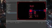
Highlighting nets will help you simplify your schematic and PCB design. In Altium , there are multiple options that enable you to leverage this capability to simplify the verification of connections and circuit paths and make sure that the design you send to your manufacturer accurately reflects the printed circuit board you need built.

Read More
Blog • May 12, 2020
Keep Your Altium Designer PCB Layout in Line with Grids and Grid-Selection Shortcuts

The grid system in a printed circuit board design CAD system really is your friend, and if you haven’t taken the time to get properly introduced yet let me help you with that.

Read More
Article preview
Blog • May 7, 2020
How to Panelize Your PCBs Before Lunch with Altium Designer

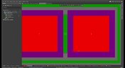
Whether you have a slew of PCBs to mass produce for your customers or a handful of project boards you wish to prototype all in one simple swoop, panelization is an effective way to bring high amounts of efficiency to your production.

Read More
Routed tracks
Blog • May 5, 2020
Helpful Tips for Interactive Routing in Altium Designer

Before you jump into the software, you should know the types of things you’re going to want to look out for. Traces, connection lines, differential pair routing, and route paths can all affect the routing process of your board. Make sure that you’re equipped knowing, ultimately, what you want your board design to accomplish and furthermore, where you anticipate potential problem areas to be.

Read More
Altium 365 + Altium Designer 20.1 Available Now!
Blog • May 1, 2020
Altium 365 + Altium Designer 20.1 Released Today - Work from Anywhere, Connect with Anyone
In our efforts to bring the best experience to the PCB design process, we are proud to announce the release of Altium Designer 20.1, Altium 365, and Altium NEXUS Client 3.1. This release enhances the design experience by bringing the convenience and benefits of the Altium 365 cloud platform to Altium Designer.
Read More
Blog • Apr 27, 2020
Introduction to High Speed PCB Designing: How to Eliminate Crosstalk

Crosstalk on your PCB layout can be disastrous. If not corrected, crosstalk can cause your finished circuit board to either not work at all, or it may be plagued by intermittent problems. Let’s take a look at what crosstalk is and what you can do to prevent it.

Read More
Blog • Apr 22, 2020
Any Angle Routing: When Should You Use It?

EDA tools have come a long way since the advent of personal computing. Now advanced routing features like auto-routers, interactive routing, length tuning, and pin-swapping are helping designers stay productive, especially as device and trace densities increase. Read full article in our blog:

Read More
Blog • Mar 20, 2020
A Message from Altium on COVID-19

We understand that many of you, like ourselves, have transitioned to working remotely. This process comes with its challenges and we would like to offer all and any help we can to minimize disruptions for your teams and business.

Read More
Blog • Mar 2, 2020
About Altium Designer Home Page

With the new Altium Designer Home page, we are aiming to help users stay up to date with the latest features and productivity tricks available in Altium Designer. Learn more about the Home page in this documentation article.

Read More
altium-community-forum
Blog • Feb 25, 2020
Getting Connected: Altium’s User Community Forums

The Altium design environment is a complex and sophisticated set of software tools. Not surprisingly, becoming proficient with these tools will take some time, and you’ll need to practice every step of the design process from beginning to end. So what happens if you get stuck along the way?

Read More
Tag (field_common_tag)
Embedded thumbnail for High Speed: XSignals
How-To's • Jan 19, 2023
High Speed: XSignals

You can create, configure, and utilize xSignals in Altium Designer to make your design process more efficient and effective. We’ll show you how to do it manually, using the more comprehensive Create xSignals command, and using the xSignal wizard.

Start Watching
Embedded thumbnail for DFM and fab cost/time constraints: What is annular ring and how to configure it
How-To's • Jan 18, 2023
DFM and fab cost/time constraints: What is annular ring and how to configure it

The minimum dimension from the wall of the aperture to the edge of the pad is called an annular ring, and we can configure it with Altium Designer. We’ll show you how to get started and manage the annular ring in your design rules.

Start Watching
Embedded thumbnail for Altium 365 Getting Started: Gerber Compare
How-To's • Jan 16, 2023
Altium 365 Getting Started: Gerber Compare

The task of comparing different versions of manufacturing files usually arises when the electrical engineer needs to check and confirm the manufacturer's edits or clarify details of changes before starting production. In Altium 365 you can perform an automatic comparison of Gerber files.

Start Watching
Embedded thumbnail for Installing and Licensing Altium Designer
AD Get Started • Jan 9, 2023
Installing and Licensing Altium Designer
  • Altium Live Account
  • Downloading and Installing Altium Designer
  • Licensing Your Altium Designer
  • Activating Altium 365 Workspace
Start Watching
Embedded thumbnail for Video Series Introduction
AD Get Started • Jan 9, 2023
Video Series Introduction
  • Introduction of Altium Designer and Overview of the Next Modules
  • Presentation of Resources and Links to Help You Start with Altium Designer
Start Watching
Embedded thumbnail for New Project, Configuration, and Unified Environment
AD Get Started • Jan 9, 2023
New Project, Configuration, and Unified Environment
  • Unified Environment Platform
  • Configuration and Settings
  • Starting a New Project
Start Watching
Embedded thumbnail for Output Job File and Project Releaser
AD Get Started • Jan 9, 2023
Output Job File and Project Releaser
Output Job File
  • Output Job File Output Documents
  • Output Job File Environment, Outputs, and Output Containers
  • Generation of Output Job Files
Project Releaser
  • Initiating Project Release Environment
  • Preparation and Setup
  • Execution of the Releaser and Where Files Are Located for Manufacturer Use and Sending
Start Watching
Embedded thumbnail for PCB Editor, Transferring Schematic to PCB, Design Rules, Layer Stack Manager, and Routing
AD Get Started • Jan 9, 2023
PCB Editor, Transferring Schematic to PCB, Design Rules, Layer Stack Manager, and Routing
  • Transferring Schematic to PCB Editor
  • Editor Environment and Preparation
  • Board Shape and Size
  • Layer Stack Manager
  • Design Rules
  • Board Routing
Start Watching
Embedded thumbnail for Schematic Editor and Component Usage Management and Menus
AD Get Started • Jan 9, 2023
Schematic Editor and Component Usage Management and Menus
  • Altium Designer Schematic Editor
  • Schematic Types (Hierarchical and Flat) and Adding Schematics to Your Project
  • Proper Use of Net Labels and Ports
Start Watching
Embedded thumbnail for Polygon Pours
Working with Polygons • Jan 2, 2023
Polygon Pours

Polygon pours are used to create copper geometries on your board. You can prioritize polygon pour order, hide them to make it easier to work on your board, and repour them to resolve design rule conflicts.

Start Watching
Embedded thumbnail for How to Use the MCAD CoDesigner?
How-To's • Dec 30, 2022
How to Use the MCAD CoDesigner?

This video shows how the ECAD and MCAD engineers now can communicate directly while staying within their own design environment. The MCAD engineer is able to push design information directly from their design software straight into Altium Designer. Any changes can be reviewed, accepted, or denied by the receiving party. This process of pushing and reviewing design changes is bi-directional, meaning that both the MCAD or ECAD engineer can push and review changes to the other. 

Start Watching
Embedded thumbnail for Creating Additional Snap Points Using a 3D Model
How to use Snapping • Dec 28, 2022
Creating Additional Snap Points Using a 3D Model

Demonstration of using snap points with 3D models and how they can assist in the placement of said models.

Start Watching
Embedded thumbnail for Learn how Kärcher Developed Their First Autonomous Scrubber Drier with Altium 365
Success Stories • Dec 27, 2022
Learn how Kärcher Developed Their First Autonomous Scrubber Drier with Altium 365

Watch and see how Kärcher innovates faster and develops quality products by being able to work efficiently with interdisciplinary teams across the world to maintain its standards for the highest quality.

Start Watching
Embedded thumbnail for Polygon Connect Styles
Working with Polygons • Dec 26, 2022
Polygon Connect Styles

Define how vias and pads connect to polygons with a design rule. Customize the thermal relief width, number, and rotation as well as the air gap width.

Start Watching
Embedded thumbnail for How to work with Component Classes?
How to Work with Classes • Dec 23, 2022
How to work with Component Classes?

Modern printed circuit boards can contain a large number of components, which makes them difficult to work with. In this video we will show what component classes can be on a PCB, how to create custom component classes and how they can be useful for us. 

Start Watching
Embedded thumbnail for Create and Snap to a Circular Grid (Polar Grid)
How to use Snapping • Dec 19, 2022
Create and Snap to a Circular Grid (Polar Grid)

Instructional on how to create polar grids, how to snap to them, and why you might want to use them.

Start Watching
  • Show More
Tag (field_common_tag)
Proactive Component Selection
On-Demand Webinar • May 22, 2025
Proactive Component Selection: Mitigating Manufacturing Delays Before They Happen
Most teams spend hours on component research yet still face redesigns. Learn how Altium 365 helps you make proactive, data-driven part decisions. Join SiliconExpert’s Jackie Sartin to discover smarter sourcing with real-time insights and validated alternatives.
Watch Now
Altium Enterprise
On-Demand Webinar • May 10, 2025
Streamline your customer relation with Altium 365 Enterprise
Join our webinar designed for engineers and users in EMS companies
Watch Now
PCB
On-Demand Webinar • May 1, 2025
Altium Designer Overview
Altium Designer is the #1 PCB design tool for a reason. Join us for this live webinar and get an inside look at Altium’s world-class PCB design solution. See for yourself why design teams around the globe are making the switch to Altium Designer. Register now!
Watch Now
Enterprise
On-Demand Webinar • Apr 25, 2025
Altium Customization with Scripting or Low-Code
See how scripting, low-code, no-code, and API integrations can help you work more efficiently—without extra setup or complex systems.
Watch Now
A365 Webinar: Altium BOM Portal - From PCB Design to Parts Ordering in Minutes
On-Demand Webinar • Apr 21, 2025
Altium 365 BOM Portal - From PCB Design to Parts Ordering in Minutes
Join us to learn how to reduce sourcing time by up to 70% using Altium 365 BOM Portal.
Watch Now
April 2025 COM Webinar
On-Demand Webinar • Apr 17, 2025
Advanced xSignal and Impedance Control Techniques
We are hosting a free webinar on advanced xSignal configuration and impedance control techniques in Altium Designer to help you tackle signal integrity challenges. Register now to enhance your design skills.
Watch Now
Altium Enterprise
On-Demand Webinar • Mar 25, 2025
Unlocking the full potential of your design team with Altium's enterprise solution
See how Altium's enterprise solution can help you meet your electronic product design goals
Watch Now
Transmission line
On-Demand Webinar • Mar 4, 2025
Optimizing Layer Stackup and Impedance for High-Speed PCB Design
Learn how to master the layer stack manager to efficiently create stackups, manage materials, and ensure optimal design performance.
Watch Now
Harness design
On-Demand Webinar • Mar 2, 2025
Design Smarter - Harness, Multi-board, and MCAD CoDesign in Action
Discover how the latest Harness, Multi-board, and MCAD CoDesign tools can revolutionize your PCB design workflow.
Watch Now
ADv25
On-Demand Webinar • Jan 30, 2025
6 Reasons to Switch Design Tools
Come see how Altium Designer, the industry standard for PCB design, combined with Altium 365 delivers the world’s first connected PCB design experience.
Watch Now
PCB CoDesign
On-Demand Webinar • Jan 29, 2025
Level Up Your Team's Productivity with Altium
Discover how to create an efficient, collaborative, and transparent design process for your team!
Watch Now
Assembly variants
On-Demand Webinar • Jan 9, 2025
Designing with Assembly Variants
Join us to learn best practices and get into the details about setting up variants in your designs and speeding up your project development.
Watch Now
Single layer PCB
On-Demand Webinar • Jan 8, 2025
Optimized for Success - Advanced PCB Features in Altium Designer
This webinar will show you how to use the latest PCB Layout, signal integrity analysis, and component management design tools in Altium Designer.
Watch Now
Rigid flex
On-Demand Webinar • Dec 19, 2024
How To Use Modern Rigid-Flex Substrates
Join us in this webinar where we’ll go over how you can easily create your own flex design.
Watch Now
Power Analyzer
On-Demand Webinar • Oct 29, 2024
Power Integrity Made Simple
Power Analyzer by Keysight in Altium Designer makes it easy to resolve PDN issues that arise during the board design process within a unified design environment.
Watch Now
Electronic Component Traceability
On-Demand Webinar • Oct 25, 2024
Ensuring Electronic Component Traceability From Idea to Innovation
Watch the webinar to learn how to achieve full transparency, improve collaboration, and ensure compliance throughout your entire supply chain—whether you are sourcing domestically or abroad.
Watch Now
  • Show More
Tag (field_common_tag)
Loading
Loading...
Share link
Share with
Search by Update
Version
Update
25 26 24 23 22
25.0 25.1 25.2 25.3 25.4 25.5 25.6 25.7 25.8 25.9
26.1 26.2
24.10 24.9 24.8 24.7 24.6 24.5 24.4 24.3 24.2 24.1 24.0
23.11 23.10 23.9 23.8 23.7 23.6 23.5 23.4 23.3 23.2 23.1 23.0
22.11 22.10 22.9 22.8 22.7 22.6 22.5 22.4 22.3