
Main navigation

  • Home
  • Discover
  • Learning Center
  • What’s New

Second main navigation

  • Altium Community
  • Support
  • Documentation
×

Results

  • Updates
  • Blog 570
  • Video 539
  • Webinar 86
  • Playlist 53
Filters:
Tag (field_common_tag)
Blog • Oct 2, 2025
Most Common Causes of PCB Assembly Rework and Scrap

Many PCB assemblies fail not because of exotic faults, but due to basic issues like incorrect BOM entries or footprint mismatches that force rework or scrap. This article dives into the most common causes and how to prevent costly defects in your design-to-manufacturing process.

Read More
Embedded thumbnail for Mechanically Drilled Blind & Buried Vias: PCB Design Rules Explained
How-To's • Oct 1, 2025
Mechanically Drilled Blind & Buried Vias: PCB Design Rules Explained

Discover the essential design rules and manufacturing processes for mechanically drilled blind and buried vias in PCB layouts in this comprehensive tutorial. We cover the stack drill-and-plate fabrication process, aspect ratio limitations, sub-lamination design, and copper weight considerations. You’ll also learn how these vias differ from HDI microvias and gain a clear understanding of the critical design constraints needed for successful PCB manufacturing.

Start Watching
Blog • Sep 30, 2025
Behind the Scenes with AI Embedded Development

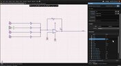
Forget one-shot AI hacks Ari Mahpour shows the thoughtful, sustainable way to integrate AI into embedded firmware development. Learn the core principles (planning gate, HAL abstraction, observability, timeout design) that can help you push your efficiency 5-10 times in real hardware projects.

Read More
Embedded thumbnail for Altium Training - Design Environment: Navigation with Schematic Workspace
Altium Training • Sep 29, 2025
Altium Training - Design Environment: Navigation with Schematic Workspace

Discover the most important navigation techniques for the schematic workspace using both mouse and keyboard controls. In this tutorial video, you’ll learn how to use the View menu commands for document fitting, area zooming, and object selection, along with advanced navigation shortcuts. Master mouse-based panning and zooming, explore Ctrl key combinations, and practice arrow key movements - all designed to simplify your workflow in the PCB design process.

Start Watching
Blog • Sep 25, 2025
We're heading to PCB West 2025!

Join Altium at PCB West 2025 in Santa Clara, CA, on October 1! Stop by Booth 300 for the official launch of the new Altium platform, built on the foundation of Altium Designer and Altium 365. Be sure to check out our live demos of Altium Develop and Altium Agile.

Read More
Blog • Sep 24, 2025
Peak Electrical Performance in Multi-Board Designs With Advanced Simulation and Compliance Tools

Moving from single-board to multi-board systems is a leap in complexity. You must manage not just routing, but power, signal integrity, mechanical fit, and regulatory requirements across boards. In this article, you’ll discover how Altium’s advanced simulation and compliance tools help engineering teams overcome these challenges and deliver reliable multi-board solutions.

Read More
Embedded thumbnail for Altium Training - Design Environment: The Altium Environment
How-To's • Sep 23, 2025
Altium Training - Design Environment: The Altium Environment

Get familiar with the core workspace layout and navigation methods. In this video, you’ll see how to open schematic and PCB documents, work within the unified design environment, and move between multiple open files using document tabs and keyboard shortcuts.

Start Watching
Blog • Sep 22, 2025
How to Catch Enclosure and Connector Misalignment Before the First Prototype

As electronics continue to miniaturize and functionality increases, even minor misalignments between enclosures and connectors can derail a project. This article explores how early integration of ECAD and MCAD workflows helps detect and eliminate those costly issues before the first prototype is built.

Read More
Embedded thumbnail for Altium Training - Design Environment: Opening a Project from a Local Drive
Altium Training • Sep 18, 2025
Altium Training - Design Environment: Opening a Project from a Local Drive

Get your PCB design workflow off to a smooth start. This Altium tutorial walks you through opening projects from your local directory - a core skill that keeps your process efficient and organized from day one.

Start Watching
Blog • Sep 17, 2025
Executive Insights Into Electronic Product Development Gaps You Need To Close

Electronics hardware development is falling behind broader product development disciplines due to fragmented workflows, poor collaboration, and limited compliance visibility. This gap introduces risk, delays, and missed opportunities but executives see real business value in modernizing electronics development through better integration, traceability, and lifecycle visibility.

Read More
Embedded thumbnail for Altium Essentials: Design Environment
Altium Training • Sep 16, 2025
Altium Essentials: Design Environment

Take control of your PCB design workflow with Altium Essentials: Design Environment. This tutorial module guides you through the fundamentals of workspace management, from handling panels and documents to mastering menus, context commands, and time-saving shortcuts.

Start Watching
Blog • Sep 15, 2025
Sourcing For High-Mix Low-Volume Electronics Manufacturing

High-mix, low-volume (HMLV) electronics manufacturing requires agile sourcing strategies to handle shifting BOMs, erratic lead times, and component volatility. All while controlling costs and ensuring compliance. Cloud-based tools like Altium provide real-time component visibility, BOM collaboration, and supplier integrations to help navigate HMLV complexities.

Read More
Embedded thumbnail for What Makes a Great PCB Design Review Submission?
How-To's • Sep 11, 2025
What Makes a Great PCB Design Review Submission?

Turn your PCB designs into professional-grade submissions. At Altium, we reveal the key practices that transform schematics, layouts, and documentation into review-ready work that stands out. Watch our brand-new tutorial and take your PCB design process to the next level.

Start Watching
Blog • Sep 10, 2025
How to Solve Fit, Form, and Function Challenges in Robotics with ECAD-MCAD Collaboration

As robotics systems become increasingly miniaturized and intricate, ensuring perfect fit, form, and function across electrical and mechanical domains is critical to avoid design setbacks. Real-time ECAD-MCAD integration with two-way sync empowers teams to streamline workflows, reduce PCB rework, and deliver more reliable designs faster.

Read More
Embedded thumbnail for Altium Training - Workspace Folder Structure: Opening the Explorer Panel
Altium Training • Sep 9, 2025
Altium Training - Workspace Folder Structure: Opening the Explorer Panel

Discover the key ways to access the Explorer panel in Altium Designer with this step-by-step tutorial. The video walks you through four different methods, giving you the freedom to choose the approach that best fits your workflow.

Start Watching
Blog • Sep 8, 2025
One Vision, Three Powerful Solutions: Introducing Altium Discover, Altium Develop, and Altium Agile

We are excited to announce the launch of three new platform-based solutions that will transform the way electronic products are designed, built, and delivered: Altium Discover, Altium Develop, and Altium Agile. These solutions are designed to simplify processes, accelerate innovation, and make collaboration seamless across the entire electronics lifecycle. Together, they realize the purpose of Altium and Renesas: To Make Our Lives Easier.

Read More
  • Show More
Tag (field_common_tag)
Blog • Jul 2, 2025
PCB First-Pass Yield: Small Decisions That Make a Big Difference

This article highlights how seemingly minor layout choices like trace spacing, component footprints, or stack-up details can dramatically impact whether a board passes fabrication and assembly the first time.

Read More
Blog • Jul 1, 2025
Implementing Design for Supply Chain Principles in Electronic Product Development

Designing with supply chain principles in mind helps you avoid delays, reduce costs, and ensure manufacturability. This article outlines practical strategies for component selection, sourcing, and lifecycle management to make your designs more resilient and production-ready.

Read More
Blog • Jun 27, 2025
Beyond the BOM: How Proactive Component Selection Is Transforming Workflows

Learn how proactive component selection helps you avoid supply chain risks, reduce costs, and design more reliably. Our new article outlines key strategies and shows how tools like Altium 365 support smarter part decisions.

Read More
Blog • Jun 26, 2025
Power Integrity Issues?

Power problems can be hard to spot until it’s too late. See how easy it is to analyze your power nets, check voltage drops, and improve reliability with Power Analyzer by Keysight - all without leaving your design environment.

Read More
Blog • Jun 24, 2025
How to Design High-Speed PCBs Without Signal Surprises

Signal issues can sneak in early and cost you later. Read our whitepaper to see how Signal Analyzer by Keysight (inside Altium Designer) helps you catch problems fast and design with confidence.

Read More
Blog • Jun 18, 2025
Beyond Basic Part Selection: Using Supply Chain Data to Validate Choices

Learn how to enhance part selection by using real-time supply chain data. This article shows how integrating insights like availability and lifecycle status helps you make smarter, risk-aware design choices.

Read More
Blog • Jun 17, 2025
Signal Mistakes Are Expensive

See how the Signal Analyzer by Keysight in Altium Designer lets you run signal integrity checks directly within your design environment. Read our article to learn how to effectively manage impedance, return paths, stackups, and more.

Read More
Blog • Jun 12, 2025
Twice the Insight. One Seamless Simulation Bundle

Ensure power and signal integrity with the Keysight Bundle in Altium Designer. Catch issues early, reduce rework, and optimize your PCBs - all within one integrated environment featuring Signal & Power Analyzer.

Read More
Blog • Jun 3, 2025
Preparing for Prototype: Final Component Validation

Final component validation is the last critical check before building a prototype, ensuring all parts are accurate, available, and viable. This article shows how Altium’s integrated tools—like SiliconExpert, Z2Data, Octopart, and BOM Portal—help teams avoid costly surprises and prepare with confidence.

Read More
Blog • Jun 2, 2025
Getting Started with Harness Design in Altium Designer 25

Explore the essential steps and tools for Harness Design in Altium Designer 25, from initial setup to final documentation. The article highlights how the unified design environment streamlines the entire process, improving efficiency and project integration.

Read More
Blog • May 30, 2025
The Future of PCB Design Starts Here

Altium Designer is constantly evolving, with powerful new features and updates on the way. Get an exclusive first look at what’s coming next—visit our Coming Soon page to stay up to date with the latest innovations.

Read More
Blog • May 29, 2025
Simplify Harness-to-System Connections for Better PCB Design Outcomes

Struggling to keep harness and system designs in sync? In our brand-new article we explore how integrating PCB and harness design workflows can eliminate errors, improve collaboration, and accelerate your development process. Discover a smarter approach to connecting your harness to the system.

Read More
Blog • May 27, 2025
The Crucial Balance: Cost, Quality, and Availability In Electronic Component Selection

Balancing cost, quality, and availability is key when selecting electronic components. This article explores how to make informed choices that meet design goals while managing supply chain and sourcing challenges.

Read More
Blog • May 19, 2025
Wire Harness Failures: The Hidden Costs and Real-World Recalls That Could Have Been Prevented

Wire harness failures can lead to significant financial losses, production delays, and safety hazards. This article delves into real-world examples of such failures across industries and illustrates how modern CAD tools can help prevent these costly issues.

Read More
Blog • May 13, 2025
Part Selection Fundamentals: Creating Resilient Component Requirements

Learn how to ensure electronic components meet the demands of harsh environments. This article explores key standards, testing protocols, and design considerations for building resilient systems that perform reliably under extreme conditions.

Read More
Blog • May 12, 2025
Printed Electronics: The Future of Flexible and Cost-Effective Circuit Design

This article explores the rise of printed electronics as a lightweight, flexible, and cost-effective alternative to traditional PCB design. It highlights key benefits like reduced manufacturing costs, sustainability, and new design possibilities—especially in wearables, medical devices, and automotive applications. 

Read More
  • Show More
Tag (field_common_tag)
Embedded thumbnail for Buck Converter
Simulation in Altium Designer • Sep 25, 2023
Buck Converter

Learn how to run a transient simulation, analyze the waveforms, and measurement techniques you can use to determine a voltage ripple with a buck converter as an example. 

Start Watching
Embedded thumbnail for Edge Plating in RF Design
How-To's • Sep 21, 2023
Edge Plating in RF Design

PCB Edge Plating provides additional noise suppression and improves EMC. In this video we provide you some practical tips for creating metalized PCB edges in Altium Designer.

Start Watching
Embedded thumbnail for Custom Paste Mask and Solder Mask
Custom Pad Stack in Altium Designer • Sep 19, 2023
Custom Paste Mask and Solder Mask

Altium Designer allows you to freely customize paste and solder mask shapes, which allows you to adapt your design for non-standard component footprints.

Start Watching
Embedded thumbnail for Colpitts Oscillator
Simulation in Altium Designer • Sep 15, 2023
Colpitts Oscillator

Learn how to effectively fix errors in circuit simulation and other problem-solving techniques using a Colpitts Oscillator design as an example. 

Start Watching
Embedded thumbnail for Custom Thermal Reliefs for Pads
Custom Pad Stack in Altium Designer • Sep 12, 2023
Custom Thermal Reliefs for Pads

Altium Designer allows you to add, remove, and edit thermal relief spikes anywhere on a pad, regardless of its shape. Using these can improve soldering and prevent manufacturing problems like tombstoning.

Start Watching
Embedded thumbnail for Notch Filter
Simulation in Altium Designer • Sep 8, 2023
Notch Filter

Learn how to run an AC sweep analysis, execute a Monte Carlo simulation, and interpret the results using a notch filter as an example. 

Start Watching
Embedded thumbnail for Custom Pad Shapes
Custom Pad Stack in Altium Designer • Sep 5, 2023
Custom Pad Shapes

Modern components often contain pads with complex shapes. Altium Designer allows you to create custom pad shapes quickly and easily, and manage them like you would a standard pad.

Start Watching
Embedded thumbnail for Low-Pass Filter
Simulation in Altium Designer • Aug 30, 2023
Low-Pass Filter

Learn how to modify an op amp low-pass filter circuit for simulation. 

Start Watching
Embedded thumbnail for Design Reuse
How-To's • Aug 29, 2023
Design Reuse

If you need to shorten your time-to-market, reduce costs, and minimize errors in the design process. Then you need to make sure that you’re designing smarter, with design reuse blocks. Check out this demo to see how it works.

Start Watching
Embedded thumbnail for Flyback Converter
Simulation in Altium Designer • Aug 25, 2023
Flyback Converter

Learn how to use transient analysis on an example flyback converter and handle basic errors during the simulation preparation. 

Start Watching
Embedded thumbnail for Analog to Digital Converter
Simulation in Altium Designer • Aug 21, 2023
Analog to Digital Converter

Learn how to run a mixed-signal (analog and digital) design simulation.

Start Watching
Embedded thumbnail for Back Drilling in Altium Designer
How-To's • Aug 18, 2023
Back Drilling in Altium Designer

In this video, we will learn about Back Drilling technology, how to set up back drilling using the Layer Stack Manager, and how to set up the Stub Length sizes for back drilling by specifying applicable nets using the Design Rules Editor.

Start Watching
Embedded thumbnail for Distributed - Element Circuits in RF Design
How-To's • Aug 16, 2023
Distributed - Element Circuits in RF Design

The capacitance and inductance of Distributed-Element circuits are determined by the shape and location of different copper elements in the PCB layout, instead of being concentrated in one point in space. Learn how to work with these circuits in Altium Designer.

Start Watching
Embedded thumbnail for Collaborative Editing
How-To's • Aug 10, 2023
Collaborative Editing

Save time and minimize reworks while teaming up on a PCB design from anywhere in the world. Watch the video for a sneak preview of the new collaborative editing functionality.

Start Watching
Embedded thumbnail for Exporting Results
How To Work with Power Analyzer by Keysight • Aug 8, 2023
Exporting Results

After completing your simulation in Power Analyzer by Keysight, you will likely need to export some of the results for further analysis. In this video, we will show you how to prepare a report once the simulation is done.

Start Watching
Embedded thumbnail for Plane Connect - Direct in RF Design
How-To's • Aug 3, 2023
Plane Connect - Direct in RF Design

Designing high-frequency circuit boards requires a sharp eye toward maintaining signal integrity. Some signal connections are more prone to interruption than others. In this video, you can learn how Altium Designer's Polygon Connect Design Rule and the Thermal Relief option can help in the PCB design process.

Start Watching
  • Show More
Tag (field_common_tag)
Altium Enterprise
On-Demand Webinar • May 10, 2025
Streamline your customer relation with Altium 365 Enterprise
Join our webinar designed for engineers and users in EMS companies
Watch Now
PCB
On-Demand Webinar • May 1, 2025
Altium Designer Overview
Altium Designer is the #1 PCB design tool for a reason. Join us for this live webinar and get an inside look at Altium’s world-class PCB design solution. See for yourself why design teams around the globe are making the switch to Altium Designer. Register now!
Watch Now
Enterprise
On-Demand Webinar • Apr 25, 2025
Altium Customization with Scripting or Low-Code
See how scripting, low-code, no-code, and API integrations can help you work more efficiently—without extra setup or complex systems.
Watch Now
A365 Webinar: Altium BOM Portal - From PCB Design to Parts Ordering in Minutes
On-Demand Webinar • Apr 21, 2025
Altium 365 BOM Portal - From PCB Design to Parts Ordering in Minutes
Join us to learn how to reduce sourcing time by up to 70% using Altium 365 BOM Portal.
Watch Now
April 2025 COM Webinar
On-Demand Webinar • Apr 17, 2025
Advanced xSignal and Impedance Control Techniques
We are hosting a free webinar on advanced xSignal configuration and impedance control techniques in Altium Designer to help you tackle signal integrity challenges. Register now to enhance your design skills.
Watch Now
Altium Enterprise
On-Demand Webinar • Mar 25, 2025
Unlocking the full potential of your design team with Altium's enterprise solution
See how Altium's enterprise solution can help you meet your electronic product design goals
Watch Now
Transmission line
On-Demand Webinar • Mar 4, 2025
Optimizing Layer Stackup and Impedance for High-Speed PCB Design
Learn how to master the layer stack manager to efficiently create stackups, manage materials, and ensure optimal design performance.
Watch Now
Harness design
On-Demand Webinar • Mar 2, 2025
Design Smarter - Harness, Multi-board, and MCAD CoDesign in Action
Discover how the latest Harness, Multi-board, and MCAD CoDesign tools can revolutionize your PCB design workflow.
Watch Now
ADv25
On-Demand Webinar • Jan 30, 2025
6 Reasons to Switch Design Tools
Come see how Altium Designer, the industry standard for PCB design, combined with Altium 365 delivers the world’s first connected PCB design experience.
Watch Now
PCB CoDesign
On-Demand Webinar • Jan 29, 2025
Level Up Your Team's Productivity with Altium
Discover how to create an efficient, collaborative, and transparent design process for your team!
Watch Now
Assembly variants
On-Demand Webinar • Jan 9, 2025
Designing with Assembly Variants
Join us to learn best practices and get into the details about setting up variants in your designs and speeding up your project development.
Watch Now
Single layer PCB
On-Demand Webinar • Jan 8, 2025
Optimized for Success - Advanced PCB Features in Altium Designer
This webinar will show you how to use the latest PCB Layout, signal integrity analysis, and component management design tools in Altium Designer.
Watch Now
Rigid flex
On-Demand Webinar • Dec 19, 2024
How To Use Modern Rigid-Flex Substrates
Join us in this webinar where we’ll go over how you can easily create your own flex design.
Watch Now
Power Analyzer
On-Demand Webinar • Oct 29, 2024
Power Integrity Made Simple
Power Analyzer by Keysight in Altium Designer makes it easy to resolve PDN issues that arise during the board design process within a unified design environment.
Watch Now
Electronic Component Traceability
On-Demand Webinar • Oct 25, 2024
Ensuring Electronic Component Traceability From Idea to Innovation
Watch the webinar to learn how to achieve full transparency, improve collaboration, and ensure compliance throughout your entire supply chain—whether you are sourcing domestically or abroad.
Watch Now
Why Altium Designer is Your Next Step for PCB Design
On-Demand Webinar • Oct 24, 2024
Why Altium Designer is Your Next Step for PCB Design
Join us to see how moving to Altium Designer can enable resilient and scalable designs while streamlining your entire workflow.
Watch Now
  • Show More
Tag (field_common_tag)
Loading
Loading...
Share link
Share with
Search by Update
Version
Update
25 26 24 23 22
25.0 25.1 25.2 25.3 25.4 25.5 25.6 25.7 25.8 25.9
26.1 26.2
24.10 24.9 24.8 24.7 24.6 24.5 24.4 24.3 24.2 24.1 24.0
23.11 23.10 23.9 23.8 23.7 23.6 23.5 23.4 23.3 23.2 23.1 23.0
22.11 22.10 22.9 22.8 22.7 22.6 22.5 22.4 22.3