
Main navigation

  • Home
  • Discover
  • Learning Center
  • What’s New

Second main navigation

  • Altium Community
  • Support
  • Documentation
×

Results

  • Updates
  • Blog 571
  • Video 540
  • Webinar 86
  • Playlist 53
Filters:
Tag (field_common_tag)
Blog • Oct 7, 2025
How ECAD-MCAD Co-Design Supports Aerospace Reliability and Compliance

When the margin for error is nearly zero, aerospace engineering demands a design process that’s seamless across all domains. Here, we explore how ECAD-MCAD co-design delivers an integrated workflow that supports first-pass success and compliance with strict aerospace standards.

Read More
Embedded thumbnail for Altium Training - Design Environment: Documents and Panels
Altium Training • Oct 6, 2025
Altium Training - Design Environment: Documents and Panels

In our new tutorial, we explore different panel display modes, including docked, floating, and tabbed grouping arrangements. Effective panel management is essential for creating an efficient design environment tailored to your specific workflow requirements.

Start Watching
Blog • Oct 2, 2025
Most Common Causes of PCB Assembly Rework and Scrap

Many PCB assemblies fail not because of exotic faults, but due to basic issues like incorrect BOM entries or footprint mismatches that force rework or scrap. This article dives into the most common causes and how to prevent costly defects in your design-to-manufacturing process.

Read More
Embedded thumbnail for Mechanically Drilled Blind & Buried Vias: PCB Design Rules Explained
How-To's • Oct 1, 2025
Mechanically Drilled Blind & Buried Vias: PCB Design Rules Explained

Discover the essential design rules and manufacturing processes for mechanically drilled blind and buried vias in PCB layouts in this comprehensive tutorial. We cover the stack drill-and-plate fabrication process, aspect ratio limitations, sub-lamination design, and copper weight considerations. You’ll also learn how these vias differ from HDI microvias and gain a clear understanding of the critical design constraints needed for successful PCB manufacturing.

Start Watching
Blog • Sep 30, 2025
Behind the Scenes with AI Embedded Development

Forget one-shot AI hacks Ari Mahpour shows the thoughtful, sustainable way to integrate AI into embedded firmware development. Learn the core principles (planning gate, HAL abstraction, observability, timeout design) that can help you push your efficiency 5-10 times in real hardware projects.

Read More
Embedded thumbnail for Altium Training - Design Environment: Navigation with Schematic Workspace
Altium Training • Sep 29, 2025
Altium Training - Design Environment: Navigation with Schematic Workspace

Discover the most important navigation techniques for the schematic workspace using both mouse and keyboard controls. In this tutorial video, you’ll learn how to use the View menu commands for document fitting, area zooming, and object selection, along with advanced navigation shortcuts. Master mouse-based panning and zooming, explore Ctrl key combinations, and practice arrow key movements - all designed to simplify your workflow in the PCB design process.

Start Watching
Blog • Sep 25, 2025
We're heading to PCB West 2025!

Join Altium at PCB West 2025 in Santa Clara, CA, on October 1! Stop by Booth 300 for the official launch of the new Altium platform, built on the foundation of Altium Designer and Altium 365. Be sure to check out our live demos of Altium Develop and Altium Agile.

Read More
Blog • Sep 24, 2025
Peak Electrical Performance in Multi-Board Designs With Advanced Simulation and Compliance Tools

Moving from single-board to multi-board systems is a leap in complexity. You must manage not just routing, but power, signal integrity, mechanical fit, and regulatory requirements across boards. In this article, you’ll discover how Altium’s advanced simulation and compliance tools help engineering teams overcome these challenges and deliver reliable multi-board solutions.

Read More
Embedded thumbnail for Altium Training - Design Environment: The Altium Environment
How-To's • Sep 23, 2025
Altium Training - Design Environment: The Altium Environment

Get familiar with the core workspace layout and navigation methods. In this video, you’ll see how to open schematic and PCB documents, work within the unified design environment, and move between multiple open files using document tabs and keyboard shortcuts.

Start Watching
Blog • Sep 22, 2025
How to Catch Enclosure and Connector Misalignment Before the First Prototype

As electronics continue to miniaturize and functionality increases, even minor misalignments between enclosures and connectors can derail a project. This article explores how early integration of ECAD and MCAD workflows helps detect and eliminate those costly issues before the first prototype is built.

Read More
Embedded thumbnail for Altium Training - Design Environment: Opening a Project from a Local Drive
Altium Training • Sep 18, 2025
Altium Training - Design Environment: Opening a Project from a Local Drive

Get your PCB design workflow off to a smooth start. This Altium tutorial walks you through opening projects from your local directory - a core skill that keeps your process efficient and organized from day one.

Start Watching
Blog • Sep 17, 2025
Executive Insights Into Electronic Product Development Gaps You Need To Close

Electronics hardware development is falling behind broader product development disciplines due to fragmented workflows, poor collaboration, and limited compliance visibility. This gap introduces risk, delays, and missed opportunities but executives see real business value in modernizing electronics development through better integration, traceability, and lifecycle visibility.

Read More
Embedded thumbnail for Altium Essentials: Design Environment
Altium Training • Sep 16, 2025
Altium Essentials: Design Environment

Take control of your PCB design workflow with Altium Essentials: Design Environment. This tutorial module guides you through the fundamentals of workspace management, from handling panels and documents to mastering menus, context commands, and time-saving shortcuts.

Start Watching
Blog • Sep 15, 2025
Sourcing For High-Mix Low-Volume Electronics Manufacturing

High-mix, low-volume (HMLV) electronics manufacturing requires agile sourcing strategies to handle shifting BOMs, erratic lead times, and component volatility. All while controlling costs and ensuring compliance. Cloud-based tools like Altium provide real-time component visibility, BOM collaboration, and supplier integrations to help navigate HMLV complexities.

Read More
Embedded thumbnail for What Makes a Great PCB Design Review Submission?
How-To's • Sep 11, 2025
What Makes a Great PCB Design Review Submission?

Turn your PCB designs into professional-grade submissions. At Altium, we reveal the key practices that transform schematics, layouts, and documentation into review-ready work that stands out. Watch our brand-new tutorial and take your PCB design process to the next level.

Start Watching
Blog • Sep 10, 2025
How to Solve Fit, Form, and Function Challenges in Robotics with ECAD-MCAD Collaboration

As robotics systems become increasingly miniaturized and intricate, ensuring perfect fit, form, and function across electrical and mechanical domains is critical to avoid design setbacks. Real-time ECAD-MCAD integration with two-way sync empowers teams to streamline workflows, reduce PCB rework, and deliver more reliable designs faster.

Read More
  • Show More
Tag (field_common_tag)
PCB tracks
Blog • May 6, 2021
All About Your PCB Trace Length: How Long is Too Long?

The maximum PCB trace length you can place between two components depends on multiple factors, such as signaling protocol, component specification, losses in PCB laminate, and skew. With all this in mind, let’s look at where losses accumulate along the channel.

Read More
LDO
Blog • May 4, 2021
Using an LDO vs. Switching Regulator in Your PCB

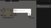
For low power devices, we generally see two types of power regulators: a low dropout regulator (LDO) or a switching regulator. You can mix and match these at different points along your power bus, but there’s still the matter of choosing whether to use an LDO vs. a switching regulator in your designs. If you’ve ever wondered how these decisions are made and when to use each type of regulator, just know that there is more to this decision than simply looking at the input/output voltage/current.

Read More
Natural flux
Blog • Apr 29, 2021
What They Don’t Teach You About Fluxes

PCB fabrication is an extremely complex technological topic that deserves recognition as the most fundamental part of PCB engineering. Unless connectors, conductive adhesive, wire-bonding, or zebra-tape are used, in the modern electronics industry it’s always necessary to use some kind of flux during the soldering process to create an electric connection. In this article, we’ll discuss fluxes — what they are, what they are made of (yes, there is going to be a lot of chemistry, don’t be scared), how they should be used, and in what direction the industry is going.

Read More
PCB with ice for best cooling
Blog • Apr 27, 2021
Thermal Management for Integrated Circuits

As anyone who designs and builds electronic devices knows, the device will generate heat when it’s switched on. Wherever current flows through an impedance, energy losses will manifest themselves as heat. Integrated circuit packaging is getting smaller to meet the trend for more compact devices but at the cost of poorer thermal properties. This article describes the basic thermal management approaches to consider in your next designs. 

Read More
Blog • Apr 22, 2021
Anatomy of Latitude Part Two: "Thread with a Needle” in the context of energy

We continue to explore the magic of energy conversion in a PWM transducer. Why is it magic? Theoretically, in a PWM transducer this happens without losses, isn't that magic? A PWM transducer, like a tailor with scissors, cuts the “fabric of energy” into pieces, and then, like a sewing machine, stitches the pieces of energy into a dress - DC Magnitude. What is a constant component and how can we get it? Let's explore!

Read More
Pulse Width Regulation Module
Blog • Apr 20, 2021
Anatomy of Latitude Part One: Pulse Width Modulation (PWM) as a Result of the Evolution of Linear Systems

There are different techniques in the world of technology to achieve various goals, both final and intermediate. Some techniques are so successful that they are commonly used with high efficiency. Electronics is no exception. The greatest example is the use of Pulse Width Modulation (PWM) signals (energy), which is applied in any modern electronic device. To apply PWM effectively, it is necessary to understand the engineering difficulties that engineers faced in the past, and the thoughts and ideas that subsequently were combined into effective, complete PWM power solutions.

Read More
Electrolytic capacitor
Blog • Apr 15, 2021
What Influences Electrolytic Capacitor Lifespan?

If you speak with a bunch of design engineers, you might quickly form the opinion that the electrolytic capacitor has a particularly dubious reputation. A faulty electrolyte mix used in these types of capacitors led to premature device failures, and quite often, a “bit of a mess” was made to the PCBs on which they were soldered. However, despite the problem of the capacitor plague, this article is focusing on helping the designer understand how to get many more years of useful life from an electrolytic capacitor.

Read More
Elegant writing
Blog • Apr 13, 2021
Creating Elegant and Readable Schematics

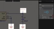
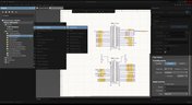
A schematic drawing will not only tell your PCB design software what needs to connect where, but it also communicates the purpose of a circuit to other people. It’s easy to create a schematic, but it can be harder to make a helpful schematic that can be quickly and easily read and comprehended by the reader. In this guide, based on years of industry experience, we will show you how to improve your schematic layout so that your designs are elegant and readable.

Read More
Copper rings
Blog • Apr 6, 2021
Must Have Rapid Prototyping Tools

Suppose your job involves rapidly iterating designs or creating a wide variety of products for clients. In that case, there are some essential tools available that can save you a tremendous amount of time, bringing high engineering risk devices to completion successfully. Whether you’re working on internal projects or developing high mix devices for clients as a consulting or freelance firm, these indispensable tools will help you ship a higher quality product in less time. 

Read More
Blog • Apr 1, 2021
Best Practices for Sharing PCB Files vs. Sharing PCB Projects

Even though today’s cloud platforms are immaculately secure and they allow a range of files to be easily shared, there are times where you should limit the data you’re sharing to only the critical files required. For PCB designers, this means either sharing entire design projects or sharing individual files with your manufacturer, customers, contractors, or collaborators. If you want to eliminate liabilities and keep your team’s design data secure, consider these best practices for sharing PCB design data with Altium 365.

Read More
Principial Schematic
Blog • Mar 30, 2021
Best Practices for Using Reference Designs

Best component companies will release reference designs for their new and legacy products to show designers an example application for a component. If the reference design is good enough and it very nicely illustrates how to quickly engineer around a few main components, I’m likely to use them in the design and the component maker has just earned my business. If you’re a newer designer and you’re wondering whether reference designs are right for your next project, follow these best practices so that you don’t make any mistakes with your reference design.

Read More
Traces on PCB
Blog • Mar 25, 2021
Transmission Line Fundamentals And Electromagnetic Fields, Part 1

When we deal with “abstract” aspects of electromagnetic fields and how they function, it can be easy to get lost in the weeds regarding them. The first part of this article will address an important aspect of transmission line fundamentals, namely how electromagnetic fields and waves propagate on a transmission line. This article’s end goal is to create a core understanding of these concepts so that when it comes time to design a PDS, the proper design methodologies are followed and a properly working PDS is achieved appropriately, the first time and every time.

Read More
BGA pads
Blog • Mar 23, 2021
Your Complete Guide to Via Stub Analysis

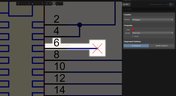
Via stubs are sometimes viewed as an annoyance, especially when you only need to make a transition between adjacent layers. For low speed, less-dense boards with low layer count, via stubs are an afterthought, or they may not receive consideration at all. For faster edge rates/higher frequencies, the conventional wisdom is to remove all via stubs. The question is: what exactly counts as “high frequency,” and how do you figure out the relevant length?

Read More
Thermal camera on people
Blog • Mar 18, 2021
Using a Thermal Camera for PCB Diagnostics

Unlike the clumsy human finger, a thermal camera can detect minute temperature differences across its view. This allows you to rapidly identify any components that are consuming current. Any parts or areas of your board that draw current will also generate heat that can easily be picked up by a thermal camera.

Read More
Soldering station
Blog • Mar 16, 2021
Complete Guide to DIY SMT Assembly In Your Office

I want to share a little secret with you in this article: Assembling SMT prototypes boards is not only easy, but it requires very little equipment. Using just a stencil, I can easily hand prototype down to 0.3 mm pitch ICs, and 0201 (imperial) sized passive components.  If you’re currently hand assembling boards with a soldering station, you need to stop this immediately and start using a stencil instead!

Read More
Road 2021
Blog • Mar 11, 2021
State of the Electronics Industry 2021

With the challenges of 2020 behind us, what challenges and opportunities lie ahead for hardware designers in 2021? In this article Vince Mazur, Technical Product Marketing Engineer at Altium, looks ahead to three emerging trends and share steps to address each one successfully in the year ahead.

Read More
  • Show More
Tag (field_common_tag)
Embedded thumbnail for New Routing Capabilities
New in Altium Designer 20 • Apr 23, 2020
New Routing Capabilities

Advanced routing capabilities help you complete the most basic, as well as the most difficult, routing challenges. In Altium Designer 20.0, we’ve added intelligent control over pad entries that are capable of working with any combination of pad geometry as well as a new any angle routing mode that allows you to make beautiful traces that smoothly contours around obstacles.

Start Watching
Embedded thumbnail for New Length Tuning Engine
New in Altium Designer 20 • Apr 21, 2020
New Length Tuning Engine

The tuning engine in Altium Designer has been redesigned and is now better than ever. Tuning sections can be picked up and moved to new locations on the track. What is truly remarkable is that the tunings are completely dynamic and change shape and fill patterns depending on the boundaries and surroundings.

Start Watching
Embedded thumbnail for Using the ActiveBOM
• Apr 20, 2020
Using the ActiveBOM

The Bill of Materials (BOM) contains a list of all the components with their designators, part numbers, values, and other parameters. An ActiveBOM manages the mapping from the design component (part) to the part that is purchased. This video descibes how to use the ActiveBOM document to create an up-to-date list of components needed for your project.

Start Watching
Embedded thumbnail for Wiring The Schematic
• Apr 20, 2020
Wiring The Schematic

This video demonstrates how to wire the schematic before it is transferred to the PCB. The Wire tool on the Active Bar or Place menu is activated and used to place wires. The video also shows how to add intermediate points along the wire route in order to more accurately route the wire.

Start Watching
Embedded thumbnail for Schematic Component Placement
• Apr 20, 2020
Schematic Component Placement

This video demonstrates how the Components panel is used to find and place components on the schematic. To search for components and filter the Components panel results, enter the component name in the Search field of the panel. The desired component appears in the filtered list and can now be placed by clicking and dragging, double-clicking on the desired component, or by right-clicking on the component then selecting Place from the context menu.

Start Watching
Embedded thumbnail for Resolving Schematic Errors
• Apr 20, 2020
Resolving Schematic Errors

So, you’ve validated your project and you’ve noticed that you have several errors and warnings, but you’re not sure where you went wrong. So we’ll be showing you some common violations, why they appeared, and how to correct them.

Start Watching
Embedded thumbnail for Searching for Errors
• Apr 20, 2020
Searching for Errors

Errors and mistakes happen to everyone - from beginners to professionals. So we always preach how its paramount for your design to be validated before pushing it to the PCB. But luckily it’s pretty easy to find and analyze any errors using Altium Designer. We’ll take a look at how to find and analyze errors in your schematic.

Start Watching
Embedded thumbnail for Schematic Port Placement
• Apr 20, 2020
Schematic Port Placement

A port is an electrical design primitive that is used to make an electrical connection between schematic sheets. The connection is made through the name of the ports on each sheet. This video shows how to place ports from the Place menu or the Active Bar, then configure the port Name, I/O Type, width, and output symbols.

Start Watching
Embedded thumbnail for Schematic Annotation
• Apr 20, 2020
Schematic Annotation

Annotation assigns designators to all or selected parts in selected sheets and ensures that designators are unique and ordered based on their position. This video demonstrates the quick and easy process for annotating schematics quietly in Altium Designer. The Annotate Schematics Quietly command used in the video applies all previous settings of the Annotate dialog without needing to reopen the dialog.

Start Watching
Embedded thumbnail for Using Net Labels
• Apr 20, 2020
Using Net Labels

Assigning names to nets has many uses, including assisting in documenting circuit design as well as providing a reference for design rules in the PCB. In this video, we demonstrate how to place net names (labels) using the Place menu. The Properties panel is then used to enter the net name.

Start Watching
Embedded thumbnail for Using Power Ports
• Apr 20, 2020
Using Power Ports

In this video, you will be shown how to place and configure power ports. Using the Power Port tool located on the Active Bar or on the Place menu, place the required power ports in the desired locations. The Properties panel can be used to set the name, style, etc., of the power port during or after placement.

Start Watching
Embedded thumbnail for Manufacturer Part Search
• Apr 20, 2020
Manufacturer Part Search

This video demonstrates how to find and place parts that are not available in your cloud or local libraries using the Manufacturer Part Search panel. The Manufacturer Part Search panel is powered by Octopart technologies and has a powerful search and filter feature based on categories and parametric filtering that allows you to zero in on the exact manufactured component you need. Once the correct part is found, you can place the part using a few clicks; you can also download or acquire the part for local use in your future designs.

Start Watching
Embedded thumbnail for Schematic Grids and Preferences
• Apr 20, 2020
Schematic Grids and Preferences

Before you start designing in the schematic environment, there are a few things you need to consider. One of those considerations would be setting your schematic grid. In this video, we'll cover how to configure different types of grids in Altium Designer.

Start Watching
Embedded thumbnail for Interaction with Projects
• Apr 20, 2020
Interaction with Projects

When you’re first starting to design your project, you should be asking yourself a few questions in regard to your project’s structure. So in this video, we’ll break down how we use a Project to represent a full design, and how we can add documents to it, such as a schematic sheet.

Start Watching
Embedded thumbnail for How to Assign Names to Polygons
Working with Polygons • Apr 3, 2020
How to Assign Names to Polygons

For some polygons, it is not always reasonable to use an automatically generated name so a custom name is needed. With a proper polygon name, you can quickly find the desired polygon in a list and correctly set the pour priority in relation to other polygons. By using unique names, you can create design rules that apply only to specified polygons.

Start Watching
Embedded thumbnail for How to Use View Mode in Altium Designer Without a License
How-To's • Mar 16, 2020
How to Use View Mode in Altium Designer Without a License

In Altium Designer 20.0, you can use Altium Designer in Viewer mode when signed into your AltiumLive account and no active license is being used. The Altium Designer Viewer license can be used by anyone with an AltiumLive account and no other licenses or subscription is needed. The license can be activated from the License Management page. 

Start Watching
  • Show More
Tag (field_common_tag)
Altium Enterprise
On-Demand Webinar • May 10, 2025
Streamline your customer relation with Altium 365 Enterprise
Join our webinar designed for engineers and users in EMS companies
Watch Now
PCB
On-Demand Webinar • May 1, 2025
Altium Designer Overview
Altium Designer is the #1 PCB design tool for a reason. Join us for this live webinar and get an inside look at Altium’s world-class PCB design solution. See for yourself why design teams around the globe are making the switch to Altium Designer. Register now!
Watch Now
Enterprise
On-Demand Webinar • Apr 25, 2025
Altium Customization with Scripting or Low-Code
See how scripting, low-code, no-code, and API integrations can help you work more efficiently—without extra setup or complex systems.
Watch Now
A365 Webinar: Altium BOM Portal - From PCB Design to Parts Ordering in Minutes
On-Demand Webinar • Apr 21, 2025
Altium 365 BOM Portal - From PCB Design to Parts Ordering in Minutes
Join us to learn how to reduce sourcing time by up to 70% using Altium 365 BOM Portal.
Watch Now
April 2025 COM Webinar
On-Demand Webinar • Apr 17, 2025
Advanced xSignal and Impedance Control Techniques
We are hosting a free webinar on advanced xSignal configuration and impedance control techniques in Altium Designer to help you tackle signal integrity challenges. Register now to enhance your design skills.
Watch Now
Altium Enterprise
On-Demand Webinar • Mar 25, 2025
Unlocking the full potential of your design team with Altium's enterprise solution
See how Altium's enterprise solution can help you meet your electronic product design goals
Watch Now
Transmission line
On-Demand Webinar • Mar 4, 2025
Optimizing Layer Stackup and Impedance for High-Speed PCB Design
Learn how to master the layer stack manager to efficiently create stackups, manage materials, and ensure optimal design performance.
Watch Now
Harness design
On-Demand Webinar • Mar 2, 2025
Design Smarter - Harness, Multi-board, and MCAD CoDesign in Action
Discover how the latest Harness, Multi-board, and MCAD CoDesign tools can revolutionize your PCB design workflow.
Watch Now
ADv25
On-Demand Webinar • Jan 30, 2025
6 Reasons to Switch Design Tools
Come see how Altium Designer, the industry standard for PCB design, combined with Altium 365 delivers the world’s first connected PCB design experience.
Watch Now
PCB CoDesign
On-Demand Webinar • Jan 29, 2025
Level Up Your Team's Productivity with Altium
Discover how to create an efficient, collaborative, and transparent design process for your team!
Watch Now
Assembly variants
On-Demand Webinar • Jan 9, 2025
Designing with Assembly Variants
Join us to learn best practices and get into the details about setting up variants in your designs and speeding up your project development.
Watch Now
Single layer PCB
On-Demand Webinar • Jan 8, 2025
Optimized for Success - Advanced PCB Features in Altium Designer
This webinar will show you how to use the latest PCB Layout, signal integrity analysis, and component management design tools in Altium Designer.
Watch Now
Rigid flex
On-Demand Webinar • Dec 19, 2024
How To Use Modern Rigid-Flex Substrates
Join us in this webinar where we’ll go over how you can easily create your own flex design.
Watch Now
Power Analyzer
On-Demand Webinar • Oct 29, 2024
Power Integrity Made Simple
Power Analyzer by Keysight in Altium Designer makes it easy to resolve PDN issues that arise during the board design process within a unified design environment.
Watch Now
Electronic Component Traceability
On-Demand Webinar • Oct 25, 2024
Ensuring Electronic Component Traceability From Idea to Innovation
Watch the webinar to learn how to achieve full transparency, improve collaboration, and ensure compliance throughout your entire supply chain—whether you are sourcing domestically or abroad.
Watch Now
Why Altium Designer is Your Next Step for PCB Design
On-Demand Webinar • Oct 24, 2024
Why Altium Designer is Your Next Step for PCB Design
Join us to see how moving to Altium Designer can enable resilient and scalable designs while streamlining your entire workflow.
Watch Now
  • Show More
Tag (field_common_tag)
Loading
Loading...
Share link
Share with
Search by Update
Version
Update
25 26 24 23 22
25.0 25.1 25.2 25.3 25.4 25.5 25.6 25.7 25.8 25.9
26.1 26.2
24.10 24.9 24.8 24.7 24.6 24.5 24.4 24.3 24.2 24.1 24.0
23.11 23.10 23.9 23.8 23.7 23.6 23.5 23.4 23.3 23.2 23.1 23.0
22.11 22.10 22.9 22.8 22.7 22.6 22.5 22.4 22.3