
Main navigation

  • Home
  • Discover
  • Learning Center
  • What’s New

Second main navigation

  • Altium Community
  • Support
  • Documentation
×

Results

  • Updates
  • Blog 570
  • Video 540
  • Webinar 86
  • Playlist 53
Filters:
Tag (field_common_tag)
Embedded thumbnail for Altium Training - Design Environment: Documents and Panels
Altium Training • Oct 6, 2025
Altium Training - Design Environment: Documents and Panels

In our new tutorial, we explore different panel display modes, including docked, floating, and tabbed grouping arrangements. Effective panel management is essential for creating an efficient design environment tailored to your specific workflow requirements.

Start Watching
Blog • Oct 2, 2025
Most Common Causes of PCB Assembly Rework and Scrap

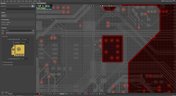
Many PCB assemblies fail not because of exotic faults, but due to basic issues like incorrect BOM entries or footprint mismatches that force rework or scrap. This article dives into the most common causes and how to prevent costly defects in your design-to-manufacturing process.

Read More
Embedded thumbnail for Mechanically Drilled Blind & Buried Vias: PCB Design Rules Explained
How-To's • Oct 1, 2025
Mechanically Drilled Blind & Buried Vias: PCB Design Rules Explained

Discover the essential design rules and manufacturing processes for mechanically drilled blind and buried vias in PCB layouts in this comprehensive tutorial. We cover the stack drill-and-plate fabrication process, aspect ratio limitations, sub-lamination design, and copper weight considerations. You’ll also learn how these vias differ from HDI microvias and gain a clear understanding of the critical design constraints needed for successful PCB manufacturing.

Start Watching
Blog • Sep 30, 2025
Behind the Scenes with AI Embedded Development

Forget one-shot AI hacks Ari Mahpour shows the thoughtful, sustainable way to integrate AI into embedded firmware development. Learn the core principles (planning gate, HAL abstraction, observability, timeout design) that can help you push your efficiency 5-10 times in real hardware projects.

Read More
Embedded thumbnail for Altium Training - Design Environment: Navigation with Schematic Workspace
Altium Training • Sep 29, 2025
Altium Training - Design Environment: Navigation with Schematic Workspace

Discover the most important navigation techniques for the schematic workspace using both mouse and keyboard controls. In this tutorial video, you’ll learn how to use the View menu commands for document fitting, area zooming, and object selection, along with advanced navigation shortcuts. Master mouse-based panning and zooming, explore Ctrl key combinations, and practice arrow key movements - all designed to simplify your workflow in the PCB design process.

Start Watching
Blog • Sep 25, 2025
We're heading to PCB West 2025!

Join Altium at PCB West 2025 in Santa Clara, CA, on October 1! Stop by Booth 300 for the official launch of the new Altium platform, built on the foundation of Altium Designer and Altium 365. Be sure to check out our live demos of Altium Develop and Altium Agile.

Read More
Blog • Sep 24, 2025
Peak Electrical Performance in Multi-Board Designs With Advanced Simulation and Compliance Tools

Moving from single-board to multi-board systems is a leap in complexity. You must manage not just routing, but power, signal integrity, mechanical fit, and regulatory requirements across boards. In this article, you’ll discover how Altium’s advanced simulation and compliance tools help engineering teams overcome these challenges and deliver reliable multi-board solutions.

Read More
Embedded thumbnail for Altium Training - Design Environment: The Altium Environment
How-To's • Sep 23, 2025
Altium Training - Design Environment: The Altium Environment

Get familiar with the core workspace layout and navigation methods. In this video, you’ll see how to open schematic and PCB documents, work within the unified design environment, and move between multiple open files using document tabs and keyboard shortcuts.

Start Watching
Blog • Sep 22, 2025
How to Catch Enclosure and Connector Misalignment Before the First Prototype

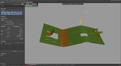
As electronics continue to miniaturize and functionality increases, even minor misalignments between enclosures and connectors can derail a project. This article explores how early integration of ECAD and MCAD workflows helps detect and eliminate those costly issues before the first prototype is built.

Read More
Embedded thumbnail for Altium Training - Design Environment: Opening a Project from a Local Drive
Altium Training • Sep 18, 2025
Altium Training - Design Environment: Opening a Project from a Local Drive

Get your PCB design workflow off to a smooth start. This Altium tutorial walks you through opening projects from your local directory - a core skill that keeps your process efficient and organized from day one.

Start Watching
Blog • Sep 17, 2025
Executive Insights Into Electronic Product Development Gaps You Need To Close

Electronics hardware development is falling behind broader product development disciplines due to fragmented workflows, poor collaboration, and limited compliance visibility. This gap introduces risk, delays, and missed opportunities but executives see real business value in modernizing electronics development through better integration, traceability, and lifecycle visibility.

Read More
Embedded thumbnail for Altium Essentials: Design Environment
Altium Training • Sep 16, 2025
Altium Essentials: Design Environment

Take control of your PCB design workflow with Altium Essentials: Design Environment. This tutorial module guides you through the fundamentals of workspace management, from handling panels and documents to mastering menus, context commands, and time-saving shortcuts.

Start Watching
Blog • Sep 15, 2025
Sourcing For High-Mix Low-Volume Electronics Manufacturing

High-mix, low-volume (HMLV) electronics manufacturing requires agile sourcing strategies to handle shifting BOMs, erratic lead times, and component volatility. All while controlling costs and ensuring compliance. Cloud-based tools like Altium provide real-time component visibility, BOM collaboration, and supplier integrations to help navigate HMLV complexities.

Read More
Embedded thumbnail for What Makes a Great PCB Design Review Submission?
How-To's • Sep 11, 2025
What Makes a Great PCB Design Review Submission?

Turn your PCB designs into professional-grade submissions. At Altium, we reveal the key practices that transform schematics, layouts, and documentation into review-ready work that stands out. Watch our brand-new tutorial and take your PCB design process to the next level.

Start Watching
Blog • Sep 10, 2025
How to Solve Fit, Form, and Function Challenges in Robotics with ECAD-MCAD Collaboration

As robotics systems become increasingly miniaturized and intricate, ensuring perfect fit, form, and function across electrical and mechanical domains is critical to avoid design setbacks. Real-time ECAD-MCAD integration with two-way sync empowers teams to streamline workflows, reduce PCB rework, and deliver more reliable designs faster.

Read More
Embedded thumbnail for Altium Training - Workspace Folder Structure: Opening the Explorer Panel
Altium Training • Sep 9, 2025
Altium Training - Workspace Folder Structure: Opening the Explorer Panel

Discover the key ways to access the Explorer panel in Altium Designer with this step-by-step tutorial. The video walks you through four different methods, giving you the freedom to choose the approach that best fits your workflow.

Start Watching
  • Show More
Tag (field_common_tag)
Protected electronic device
Blog • Jun 29, 2021
What Goes Into Rugged Electronics Design?

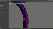
Rugged electronics need to take a punch mechanically, but there is more that goes into a rugged system than being able to survive a drop on the pavement. This is as much about enclosure design as it is about component selection and manufacturing choices. Mil-aero designers often use the term “harsh environment” to describe a number of scenarios where an electronic device’s reliability and lifetime will be put to the test. If you want to make your next product truly rugged, it helps to adopt some of their strategies in your PCB layout.

Read More
PCB Testing
Blog • Jun 24, 2021
PCB Testing 101: Important Methods and Metrics

There are many quality checks used to ensure a design will be manufacturable at scale and with high quality, but a lot of this can happen in the background without the designer realizing. No matter what level of testing and inspection you need to perform, it’s important to determine the basic test requirements your design must satisfy and communicate these to your manufacturer. If it’s your first time transitioning from prototyping to high-volume production, read our list of PCB testing requirements so that you’ll know what to expect.

Read More
DDR Memory Chip
Blog • Jun 22, 2021
Using SDRAM vs. DDR RAM in Your PCB Design

Embedded computers, vision devices, DAQ modules, and much more will all need some memory, whether it’s a Flash chip or a RAM module. Normally, something like a Flash memory chip or a small eMMC module would not be used for temporary storage as the device requires constant rewrites. Instead, if you happen to need a volatile memory solution, you would go for static (SRAM) or dynamic RAM (DRAM). If you need to decide which type of memory to use in your board, keep reading to see some of the basic design guidelines for SDRAM vs. DDR memory modules.

Read More
PCB with big ground planes
Blog • Jun 17, 2021
PCB Ground Plane Best Practices in Your Multilayer Stackup

Using a PCB ground plane in a stackup is the first step towards ensuring power and signal integrity, as well as keeping EMI low. However, there are some bad myths about ground planes that seem to persist, and I’ve seen highly experienced designers make some simple mistakes when defining grounds in their PCB layouts. If you’re interested in preventing excess emissions and ensuring signal integrity in your layout, follow these simple guidelines for implementing a PCB ground plane in your next board.

Read More
PCB Voltage Regulator Chip
Blog • Jun 15, 2021
Using an LDO vs. Switching Regulator in Your PCB

As much as we’d like, the power we supply to electronics isn’t always stable. Real power sources contain noise, they might exhibit power instability, or they dropout unexpectedly. Thankfully, we have power regulators to help prevent some of these problems. For low power devices, we generally see two types of power regulators: a low dropout regulator (LDO) or a switching regulator. You can mix and match these at different points along your power bus, but there’s still the matter of choosing whether to use an LDO vs. a switching regulator in your designs. 

Read More
Cloud storage on the phone
Blog • Jun 10, 2021
Using Altium 365 for Sharing Simulations in the Cloud

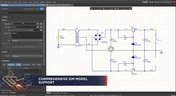
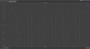
Post-layout simulators for your PCB are very valuable tools. If you’re working through a complex design, it’s a good idea to put it through some level of simulation and analysis to evaluate the design before manufacturing. This is all easy with the cloud collaboration tools in Altium 365 and Ansys field solvers thanks to the EDB Exporter utility in Altium Designer. These existing tools in Altium Designer and any of the Ansys field solver utilities give you a simplified way to share design data, EDB files, and simulation results with anyone on your design team. 

Read More
Manufacturers
Blog • Jun 8, 2021
How to Speed Up Your DFM Report Process in the Cloud

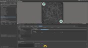
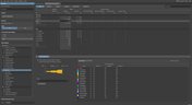
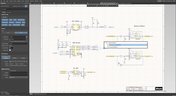
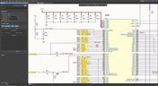
Experienced fabricators will tell you: any design could have some hidden DFM problem that will interfere with manufacturability, quality, or yield. Making use of your design rules is just the start of preventing DFM problems, you’ll want to collaborate with your manufacturer throughout the design process if you want to spot and correct DFM problems. Within Altium Designer, there are multiple reports you can generate for your projects that will help you summarize important information on your board for a client or a manufacturer.

Read More
Optoelectronics
Blog • Jun 3, 2021
The Digital Engineer's Guide to RF PCB Layout and Routing

With modern systems running at higher frequencies, incorporating multiple wireless protocols, and interfacing with many analog sensors, advanced designs require knowledge from digital and RF design disciplines. If you’re now starting to work in the RF realm and you need to design an all-analog or mixed-signal system, RF PCB layout will need to become a new specialty. If you’re a digital designer and you’re now jumping into high-frequency analog design, keep reading to learn more about RF PCB layout and routing.

Read More
Tracks on a finished PCB
Blog • Jun 1, 2021
Microstrip Ground Clearance: How Close is Too Close?

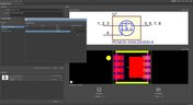
If you take a look at any guidelines for controlled impedance traces, you’ll clearly see that the trace width is calculated without any ground pour near the trace. However, most designers will state that unused areas on each PCB layer should be filled in with grounded copper pour. If you bring some ground pour near a microstrip, you’ve now formed a coplanar waveguide arrangement. So now the question becomes, how much microstrip to ground clearance do you need to ensure you’ve hit your impedance goals?

Read More
Blog • May 27, 2021
PCB Layout Guidelines for Switching Power Supplies and Regulators

In this article, I want to briefly focus on how power supplies and regulators are different, although this should already be clear to most designers. For a power supply and for a PCB with an on-board regulator, the switching regulator layout will be a major determinant of overall system performance. Therefore, we’ll largely look at some layout guidelines for switching power supplies in terms of regulator layout.

Read More
PCB Sharing - What Data You Can Share in Altium 365
Blog • May 25, 2021
PCB Sharing and What Data You Can Share in Altium 365

Altium 365 is giving design teams a new way to share and manage their design data. Most users are probably aware of project-level and component-level PCB sharing features, but sharing actually extends down to the level of individual files thanks to the managed content system within Altium 365. If you’ve ever wanted a single place to store and manage all of your design data, then Altium 365 is here to help you and your team stay organized.

Read More
Power Supply Components on PCB
Blog • May 20, 2021
How to Combat Power Supply EMI in Your PCB

Power supplies are one of those systems we all tend to take for granted. Everyone’s first task in power supply design is usually to ensure the voltage and current output reach the desired level, probably followed by thermal considerations. However, due to safety issues, EMC requirements, the use of higher PWM frequencies, and the need for smaller packaging, power supply EMI should be a major design consideration. With that being said, what are the major sources of power supply EMI, and how can power supply designers keep them in check?

Read More
Free footprint library resources
Blog • May 18, 2021
Leveraging the Free Footprint Community to Design at Lightning Speed

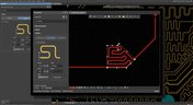
Designing footprints is a job most people hate. It’s tedious, time-consuming, and doesn’t result in much except, well, a footprint. Companies now realize this pain point and offering designers free, well-designed PCB footprints. Why would they spend their time doing this? In this article, we’re going to review some of the free offerings that exist within the PCB design community. Once you’re armed with this information, you will spend most of your time designing and routing boards instead of pulling your hair out creating footprints all day.

Read More
PCB Motherboard with Multiple Slots with RAM Memory Installed, and Other System Hardware
Blog • May 13, 2021
Designing for Multiple PCBs in the Same Project

The majority of our PCB designs sit as a single PCB under our Altium Designer projects. It sometimes happens that we have a single project that requires multiple PCBs with various stuffing options, but when it happens, a lot of us tend to get stuck. How do you handle the exact change across both projects? How do you guarantee those changes to be identical? This article will review an approach to managing multiple PCB designs within a single project, ensuring your single source of truth.

Read More
EMI and thermal challenges in 5G design
Blog • May 11, 2021
Designing 5G Devices

The next stage in the evolution of mobile telephony is here with the roll-out of 5G. The designer looking to incorporate functionality to handle 5G signals into their circuits will face some challenging issues. So, what’s so special about 5G?

Read More
PCB tracks
Blog • May 6, 2021
All About Your PCB Trace Length: How Long is Too Long?

The maximum PCB trace length you can place between two components depends on multiple factors, such as signaling protocol, component specification, losses in PCB laminate, and skew. With all this in mind, let’s look at where losses accumulate along the channel.

Read More
  • Show More
Tag (field_common_tag)
Embedded thumbnail for Using Polygons on Power Planes
New in Altium Designer 21 • Dec 28, 2020
Using Polygons on Power Planes

Traditionally, a PCB power plane is designed as a negative, that is, the objects placed on a power plane layer become voids in the copper when the board is fabricated. This approach is used because it is more efficient to generate the output data this way, as the bulk of a plane layer is normally copper; voids in the copper are only needed in specific locations such as around non-connected pads, or as separation voids when the plane is divided into different voltage regions.

Start Watching
Embedded thumbnail for Enhanced Polar Grid Support
New in Altium Designer 21 • Dec 28, 2020
Enhanced Polar Grid Support

Component placement is one of the main steps in board design. And in specific boards of a circular shape, it is convenient to use a polar grid for the location of components. Altium Designer 21 brings several improvements to the polar grid. Now, when a component is positioned in a polar grid, its properties additionally display location coordinates relative to this grid. Using them, you can quickly arrange the components in the right places. And moving the component off the grid, polar coordinates are automatically disabled.

Start Watching
Embedded thumbnail for New PCB Length Tuning Patterns
New in Altium Designer 21 • Dec 28, 2020
New PCB Length Tuning Patterns

Length matching is a critical element of high-speed design, usually solved by carefully tuning the lengths of critical routes. This release sees extensive improvements to both single-sided and differential pair length tuning capabilities. Length tuning now supports all three popular tuning patterns: Trombone, Sawtooth, and Accordion. If you are working with lower speed or lower frequency signals, you can get away with trombone tuning. For the Trombone patterns, the polygonal area that the pattern is constructed within can be thought of as a sleeve.

Start Watching
Embedded thumbnail for Expressions Library for Frequently Used Rules
New in Altium Designer 21 • Dec 28, 2020
Expressions Library for Frequently Used Rules

When working with design rules, we often use different scopes of the rules. To simplify the repetitive process of creating advanced type rules, the new Altium Designer 21 Rule Editor has the ability to save query-based object mapping scopes in a scoped library. To do this, it is enough to export the request by clicking on it with RMB. The library is presented through the Properties panel, where custom scopes can be edited, new ones added, and later reused in other custom constraint rules.

Start Watching
Embedded thumbnail for Constraint Rule Violations
New in Altium Designer 21 • Dec 28, 2020
Constraint Rule Violations

Enabled design constraint rules are applied to the current board design through a range of mechanisms, such as live Online Design Rule Checking, the batch Design Rule Checker or selectively run from the PCB Rules and Violations panel. Violations of those constraint Rules – where the specified and scoped limits are exceeded – are indicated through board graphics, panel entries and reports. With the introduction of a new Rules Editor in Altium Designer 21, violations of these rules are now displayed in the Rules Editor itself.

Start Watching
Embedded thumbnail for Table-based Approach for Design Rules and Constraints
New in Altium Designer 21 • Dec 28, 2020
Table-based Approach for Design Rules and Constraints

Define and assign a specific list of rules and constraints to all critical design elements, such as components, nets, and LVDS.

Start Watching
Embedded thumbnail for Comprehensive Simulation Model Support
New in Altium Designer 21 • Dec 28, 2020
Comprehensive Simulation Model Support

Having accurate SPICE models is critical to the success of your simulation. Altium Designer now supports analog PSpice, LTspice, and more including generic component SPICE models for when you can’t find company models. Generic components contain Spice model parameters to simplify simulation. When you are done with simulation, quickly replace your generic components with an existing component to finish your design.

Start Watching
Embedded thumbnail for Easy to Start Simulations
New in Altium Designer 21 • Dec 28, 2020
Easy to Start Simulations

0:00 Simulation Dashboard Panel Following on from the recent introduction of an advanced new SPICE Simulation engine for Altium Designer, the latest round of Simulation updates focuses on user interface. A major component of the Altium Designer Simulation user interface updates is the introduction of the Simulation Dashboard panel. The panel offers a greatly simplified approach to checking, configuring, running and reviewing simulations.

Start Watching
Embedded thumbnail for Rigid-Flex Board Planning Mode
New in Altium Designer 21 • Dec 28, 2020
Rigid-Flex Board Planning Mode

This new release of Altium Designer 21 includes significant improvements to the Rigid-Flex board designs. Along with many bug fixes and enhancements, the next phase of Altium Rigid-Flex technology development is providing functional improvements. It is now possible to create new board regions by primitives using the appropriate command from the Design » Board Shape menu. The properties of all created regions are now displayed in the Properties panel where you can edit the name of each region and define the previously created stacks for each region of the board.

Start Watching
Embedded thumbnail for Component Pin to Multiple Pad Mapping
New in Altium Designer 21 • Dec 28, 2020
Component Pin to Multiple Pad Mapping

This release introduces flexible pin to pad mapping capabilities for managed components. Enhancements to the Single Component Editor and the introduction of a new Pins panel allow component symbol pins to be mapped to any component footprint pad, or any number of footprint pads. The Pins panel, opened from the editor's button, allows the default one-to-one pin-pad mapping to be changed to a custom relationship, such as one pin being connected to multiple footprint pads – or any other non-aligned pin to pad number relationship.

Start Watching
Embedded thumbnail for Enhanced Navigation by Nets in Schematic - Altium Designer 21 What's New
New in Altium Designer 21 • Dec 28, 2020
Enhanced Navigation by Nets in Schematic - Altium Designer 21 What's New

Altium Designer 21 brings many improvements to the schematic editor aimed at visualizing circuits and improving navigation through them in multi-sheet and hierarchical designs. By holding Alt and clicking on the net, All schematic instances of the net are highlighted, while other objects are dimmed, to visibly indicate the signal/power propagation in the design using one simple action. The changes also affected the Identification of net names. Now logical and physical names of a net are displayed in the properties panel as well as when you hover over this wire.

Start Watching
Embedded thumbnail for Intelligent Schematic Insights
New in Altium Designer 21 • Dec 28, 2020
Intelligent Schematic Insights

Due to advances in the format and compilation of the Altium Designer data model, schematic Wire objects have now evolved from a simple graphical object to a more advanced form that can be directly associated with electrical parameters. As a result, the Wire mode of the Properties panel has been updated to provide an expanded set of options and a wider range of information. The new additions include a General section for net parameter options and information, and a Parameters section that lists the User Parameters, Rules and Net Classes associated with the Wire's assigned net.

Start Watching
Embedded thumbnail for Start Your Schematic with Generic Components
New in Altium Designer 21 • Dec 28, 2020
Start Your Schematic with Generic Components

It can be challenging to pick the right components when working on a new schematic. You have to consider availability, cost, and various parametric requirements. What if you could place a component to complete your design and quickly replace it when you are ready for layout? Introducing new Generic Components. Simply provide generic parameters, such as Value or Footprint, to greatly speed-up your capturing process while eliminating the need to search for specific Part Numbers or creating a needed component from scratch.

Start Watching
Embedded thumbnail for MCAD CoDesigner Overview
Working with MCAD CoDesigner extension • Dec 21, 2020
MCAD CoDesigner Overview

The MCAD CoDesigner in Altium Designer allows for seamless design transfer between the Electrical and Mechanical designers. In this overview, we’ll show you how to transfer from Altium Designer to your CAD tool of choice, then how to resize the board, add mounting holes, add a new connector, and update the board design in Altium Designer.

Start Watching
Embedded thumbnail for Bringing an MCAD Enclosure to ECAD
Working with MCAD CoDesigner extension • Nov 16, 2020
Bringing an MCAD Enclosure to ECAD

The Altium Designer MCAD CoDesigner panel and extension make it easy to move a 3D enclosure model from your MCAD tool to Altium Designer. We'll show you how and what to watch out for while your transferring your enclosure model to Altium Designer.

Start Watching
Embedded thumbnail for How to Perform a Component Search in Concord Pro - Altium Academy
How-To's • Oct 28, 2020
How to Perform a Component Search in Concord Pro - Altium Academy

In this video, I'll show you how to perform a component search in the Components Panel. Learn how to perform a component search in the Components Panel while using Altium Concord Pro to effectively host all your component libraries from Altium Designer. You can always locate any particular component using this library navigation and place it on your schematic with pricing information from global suppliers. This availability and pricing information gets updated daily directly from the suppliers so you will always get fresh, up to date information. 

Start Watching
  • Show More
Tag (field_common_tag)
Altium Enterprise
On-Demand Webinar • May 10, 2025
Streamline your customer relation with Altium 365 Enterprise
Join our webinar designed for engineers and users in EMS companies
Watch Now
PCB
On-Demand Webinar • May 1, 2025
Altium Designer Overview
Altium Designer is the #1 PCB design tool for a reason. Join us for this live webinar and get an inside look at Altium’s world-class PCB design solution. See for yourself why design teams around the globe are making the switch to Altium Designer. Register now!
Watch Now
Enterprise
On-Demand Webinar • Apr 25, 2025
Altium Customization with Scripting or Low-Code
See how scripting, low-code, no-code, and API integrations can help you work more efficiently—without extra setup or complex systems.
Watch Now
A365 Webinar: Altium BOM Portal - From PCB Design to Parts Ordering in Minutes
On-Demand Webinar • Apr 21, 2025
Altium 365 BOM Portal - From PCB Design to Parts Ordering in Minutes
Join us to learn how to reduce sourcing time by up to 70% using Altium 365 BOM Portal.
Watch Now
April 2025 COM Webinar
On-Demand Webinar • Apr 17, 2025
Advanced xSignal and Impedance Control Techniques
We are hosting a free webinar on advanced xSignal configuration and impedance control techniques in Altium Designer to help you tackle signal integrity challenges. Register now to enhance your design skills.
Watch Now
Altium Enterprise
On-Demand Webinar • Mar 25, 2025
Unlocking the full potential of your design team with Altium's enterprise solution
See how Altium's enterprise solution can help you meet your electronic product design goals
Watch Now
Transmission line
On-Demand Webinar • Mar 4, 2025
Optimizing Layer Stackup and Impedance for High-Speed PCB Design
Learn how to master the layer stack manager to efficiently create stackups, manage materials, and ensure optimal design performance.
Watch Now
Harness design
On-Demand Webinar • Mar 2, 2025
Design Smarter - Harness, Multi-board, and MCAD CoDesign in Action
Discover how the latest Harness, Multi-board, and MCAD CoDesign tools can revolutionize your PCB design workflow.
Watch Now
ADv25
On-Demand Webinar • Jan 30, 2025
6 Reasons to Switch Design Tools
Come see how Altium Designer, the industry standard for PCB design, combined with Altium 365 delivers the world’s first connected PCB design experience.
Watch Now
PCB CoDesign
On-Demand Webinar • Jan 29, 2025
Level Up Your Team's Productivity with Altium
Discover how to create an efficient, collaborative, and transparent design process for your team!
Watch Now
Assembly variants
On-Demand Webinar • Jan 9, 2025
Designing with Assembly Variants
Join us to learn best practices and get into the details about setting up variants in your designs and speeding up your project development.
Watch Now
Single layer PCB
On-Demand Webinar • Jan 8, 2025
Optimized for Success - Advanced PCB Features in Altium Designer
This webinar will show you how to use the latest PCB Layout, signal integrity analysis, and component management design tools in Altium Designer.
Watch Now
Rigid flex
On-Demand Webinar • Dec 19, 2024
How To Use Modern Rigid-Flex Substrates
Join us in this webinar where we’ll go over how you can easily create your own flex design.
Watch Now
Power Analyzer
On-Demand Webinar • Oct 29, 2024
Power Integrity Made Simple
Power Analyzer by Keysight in Altium Designer makes it easy to resolve PDN issues that arise during the board design process within a unified design environment.
Watch Now
Electronic Component Traceability
On-Demand Webinar • Oct 25, 2024
Ensuring Electronic Component Traceability From Idea to Innovation
Watch the webinar to learn how to achieve full transparency, improve collaboration, and ensure compliance throughout your entire supply chain—whether you are sourcing domestically or abroad.
Watch Now
Why Altium Designer is Your Next Step for PCB Design
On-Demand Webinar • Oct 24, 2024
Why Altium Designer is Your Next Step for PCB Design
Join us to see how moving to Altium Designer can enable resilient and scalable designs while streamlining your entire workflow.
Watch Now
  • Show More
Tag (field_common_tag)
Loading
Loading...
Share link
Share with
Search by Update
Version
Update
25 26 24 23 22
25.0 25.1 25.2 25.3 25.4 25.5 25.6 25.7 25.8 25.9
26.1 26.2
24.10 24.9 24.8 24.7 24.6 24.5 24.4 24.3 24.2 24.1 24.0
23.11 23.10 23.9 23.8 23.7 23.6 23.5 23.4 23.3 23.2 23.1 23.0
22.11 22.10 22.9 22.8 22.7 22.6 22.5 22.4 22.3