
Main navigation

  • Home
  • Discover
  • Learning Center
  • What’s New

Second main navigation

  • Altium Community
  • Support
  • Documentation
×

Results

  • Updates
  • Blog 570
  • Video 539
  • Webinar 86
  • Playlist 53
Filters:
Tag (field_common_tag)
Blog • Oct 2, 2025
Most Common Causes of PCB Assembly Rework and Scrap

Many PCB assemblies fail not because of exotic faults, but due to basic issues like incorrect BOM entries or footprint mismatches that force rework or scrap. This article dives into the most common causes and how to prevent costly defects in your design-to-manufacturing process.

Read More
Embedded thumbnail for Mechanically Drilled Blind & Buried Vias: PCB Design Rules Explained
How-To's • Oct 1, 2025
Mechanically Drilled Blind & Buried Vias: PCB Design Rules Explained

Discover the essential design rules and manufacturing processes for mechanically drilled blind and buried vias in PCB layouts in this comprehensive tutorial. We cover the stack drill-and-plate fabrication process, aspect ratio limitations, sub-lamination design, and copper weight considerations. You’ll also learn how these vias differ from HDI microvias and gain a clear understanding of the critical design constraints needed for successful PCB manufacturing.

Start Watching
Blog • Sep 30, 2025
Behind the Scenes with AI Embedded Development

Forget one-shot AI hacks Ari Mahpour shows the thoughtful, sustainable way to integrate AI into embedded firmware development. Learn the core principles (planning gate, HAL abstraction, observability, timeout design) that can help you push your efficiency 5-10 times in real hardware projects.

Read More
Embedded thumbnail for Altium Training - Design Environment: Navigation with Schematic Workspace
Altium Training • Sep 29, 2025
Altium Training - Design Environment: Navigation with Schematic Workspace

Discover the most important navigation techniques for the schematic workspace using both mouse and keyboard controls. In this tutorial video, you’ll learn how to use the View menu commands for document fitting, area zooming, and object selection, along with advanced navigation shortcuts. Master mouse-based panning and zooming, explore Ctrl key combinations, and practice arrow key movements - all designed to simplify your workflow in the PCB design process.

Start Watching
Blog • Sep 25, 2025
We're heading to PCB West 2025!

Join Altium at PCB West 2025 in Santa Clara, CA, on October 1! Stop by Booth 300 for the official launch of the new Altium platform, built on the foundation of Altium Designer and Altium 365. Be sure to check out our live demos of Altium Develop and Altium Agile.

Read More
Blog • Sep 24, 2025
Peak Electrical Performance in Multi-Board Designs With Advanced Simulation and Compliance Tools

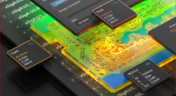
Moving from single-board to multi-board systems is a leap in complexity. You must manage not just routing, but power, signal integrity, mechanical fit, and regulatory requirements across boards. In this article, you’ll discover how Altium’s advanced simulation and compliance tools help engineering teams overcome these challenges and deliver reliable multi-board solutions.

Read More
Embedded thumbnail for Altium Training - Design Environment: The Altium Environment
How-To's • Sep 23, 2025
Altium Training - Design Environment: The Altium Environment

Get familiar with the core workspace layout and navigation methods. In this video, you’ll see how to open schematic and PCB documents, work within the unified design environment, and move between multiple open files using document tabs and keyboard shortcuts.

Start Watching
Blog • Sep 22, 2025
How to Catch Enclosure and Connector Misalignment Before the First Prototype

As electronics continue to miniaturize and functionality increases, even minor misalignments between enclosures and connectors can derail a project. This article explores how early integration of ECAD and MCAD workflows helps detect and eliminate those costly issues before the first prototype is built.

Read More
Embedded thumbnail for Altium Training - Design Environment: Opening a Project from a Local Drive
Altium Training • Sep 18, 2025
Altium Training - Design Environment: Opening a Project from a Local Drive

Get your PCB design workflow off to a smooth start. This Altium tutorial walks you through opening projects from your local directory - a core skill that keeps your process efficient and organized from day one.

Start Watching
Blog • Sep 17, 2025
Executive Insights Into Electronic Product Development Gaps You Need To Close

Electronics hardware development is falling behind broader product development disciplines due to fragmented workflows, poor collaboration, and limited compliance visibility. This gap introduces risk, delays, and missed opportunities but executives see real business value in modernizing electronics development through better integration, traceability, and lifecycle visibility.

Read More
Embedded thumbnail for Altium Essentials: Design Environment
Altium Training • Sep 16, 2025
Altium Essentials: Design Environment

Take control of your PCB design workflow with Altium Essentials: Design Environment. This tutorial module guides you through the fundamentals of workspace management, from handling panels and documents to mastering menus, context commands, and time-saving shortcuts.

Start Watching
Blog • Sep 15, 2025
Sourcing For High-Mix Low-Volume Electronics Manufacturing

High-mix, low-volume (HMLV) electronics manufacturing requires agile sourcing strategies to handle shifting BOMs, erratic lead times, and component volatility. All while controlling costs and ensuring compliance. Cloud-based tools like Altium provide real-time component visibility, BOM collaboration, and supplier integrations to help navigate HMLV complexities.

Read More
Embedded thumbnail for What Makes a Great PCB Design Review Submission?
How-To's • Sep 11, 2025
What Makes a Great PCB Design Review Submission?

Turn your PCB designs into professional-grade submissions. At Altium, we reveal the key practices that transform schematics, layouts, and documentation into review-ready work that stands out. Watch our brand-new tutorial and take your PCB design process to the next level.

Start Watching
Blog • Sep 10, 2025
How to Solve Fit, Form, and Function Challenges in Robotics with ECAD-MCAD Collaboration

As robotics systems become increasingly miniaturized and intricate, ensuring perfect fit, form, and function across electrical and mechanical domains is critical to avoid design setbacks. Real-time ECAD-MCAD integration with two-way sync empowers teams to streamline workflows, reduce PCB rework, and deliver more reliable designs faster.

Read More
Embedded thumbnail for Altium Training - Workspace Folder Structure: Opening the Explorer Panel
Altium Training • Sep 9, 2025
Altium Training - Workspace Folder Structure: Opening the Explorer Panel

Discover the key ways to access the Explorer panel in Altium Designer with this step-by-step tutorial. The video walks you through four different methods, giving you the freedom to choose the approach that best fits your workflow.

Start Watching
Blog • Sep 8, 2025
One Vision, Three Powerful Solutions: Introducing Altium Discover, Altium Develop, and Altium Agile

We are excited to announce the launch of three new platform-based solutions that will transform the way electronic products are designed, built, and delivered: Altium Discover, Altium Develop, and Altium Agile. These solutions are designed to simplify processes, accelerate innovation, and make collaboration seamless across the entire electronics lifecycle. Together, they realize the purpose of Altium and Renesas: To Make Our Lives Easier.

Read More
  • Show More
Tag (field_common_tag)
MLCC controlled ESR capacitor
Blog • Oct 19, 2021
Controlled ESR Capacitors: Should You Use Them for Power Integrity?

I can’t think of a single product I’ve built that doesn’t require capacitors. We often talk a lot about effective series inductance (ESL) in capacitors and its effects on power integrity. What about effective series resistance (ESR)? Is there a technique you can use to determine the appropriate level of resistance, and can you use ESR to your advantage?

Read More
Ground Pour, Impedance and Losses
Blog • Oct 14, 2021
Microstrip Ground Clearance Part 2: How Clearance Affects Losses

If your goal is to hit a target impedance, and you’re worried about how nearby pour might affect impedance, you can get closer than the limits set by the 3W rule. But what are the effects on losses? If the reason for this question isn’t obvious, or if you’re not up-to-date on the finer points of transmission line design, then keep reading to see how nearby ground pour can affect losses in impedance-controlled interconnects.

Read More
Choosing the Right Microphone for Embedded Applications
Blog • Oct 12, 2021
Choosing the Right Microphone for Embedded Applications

If you need to capture sound waves for your electrical device to process, you'll need a microphone. However, microphones these days have become very advanced, and there are so many options to choose from. They range from the relatively simple and popular condenser type microphones to state-of-the-art sound conversion solutions incorporating internal amplifiers and other electronic processing functionality. In this article, we'll take a look at some of the options available.

Read More
 Computer planet with circuit grid
Blog • Oct 7, 2021
Composite Amplifiers and How They Give the Best of Both Worlds

There are many times where you need an amplifier with high gain, low noise, high slew rate, and broad bandwidth simultaneously. However, not all of these design goals are possible with all off-the-shelf components. Here are some points to consider when working with a composite amplifier design and how to evaluate your design with the right set of circuit simulation tools.

Read More
Impedance balancing power supply
Blog • Oct 5, 2021
Reduce Common-Mode Noise in Your Power Supply with Impedance Balancing

Simple switching regulator circuits that operate in compact spaces, like on a small PCB, can usually be deployed in noisy environments without superimposing significant noise on the output power level. As long as you lay out the board properly, you’ll probably only need a simple filter circuit to remove EMI on the inputs and outputs. As the regulator becomes larger, both physically and electrically, noise problems can become much more apparent, namely radiated EMI and conducted EMI in the PCB layout.

Read More
Part 1: Why Your PCB Design Review Process Is Obsolete and What You Can Do About It
Blog • Sep 28, 2021
Part 1: Why Your PCB Design Review Process Is Obsolete and What You Can Do About It

A PCB design review is a practice to review the design of a board for possible errors and issues at various stages of product development. It can range from a formal checklist with official sign-offs to a more free-form inspection of schematic drawings and PCB layouts. For this article, we will not delve into what to check during a design review process but rather look at how a review process itself usually unfolds and how to optimize it to get the most out of your time.

Read More
Part 2: Why Your PCB Design Review Process Is Obsolete and What You Can Do About It
Blog • Sep 27, 2021
Part 2: Why Your PCB Design Review Process Is Obsolete and What You Can Do About It

As we established in Part 1, the PCB design review and collaboration practices have room for improvement in many organizations. To address this, we developed Altium 365. Let's examine how running a PCB project through Altium 365 compares to other methods.

Read More
Star ground PCB
Blog • Sep 23, 2021
What is PCB Star Grounding and Why Would Anyone Use It?

If you look on the internet, you'll find some interesting grounding recommendations, and sometimes terminology gets thrown around and applied to a PCB without the proper context or understanding of real electrical behavior. DC recommendations get applied to AC, low current gets applied to high current, and vice versa... the list goes on. One of the more interesting grounding techniques you'll see as a recommendation, including on some popular engineering blogs within the industry, is the use of PCB star grounding.

Read More
Silkscreen on PCB
Blog • Sep 21, 2021
Your Guide to PCB Silkscreen

Every PCB has silkscreen on the surface layer, and you’ll see a range of alphanumeric codes, numbers, markings, and logos on PCB silkscreen. What exactly does it all mean, and what specifically should you include in your silkscreen layer? All designs are different, but there are some common pieces of information that will appear in any silkscreen in order to aid assembly, testing, debug, and traceability

Read More
Gibbs ringing
Blog • Sep 16, 2021
What Causes Gibbs Ringing in High-speed Channel Simulations?

Designing high-speed channels on complex boards requires simulations, measurements on test boards, or both to ensure the design operates as you intend. Gibbs ringing is one of these effects that can occur when calculating a channel’s response using band-limited network parameters. Just as is the case in measurements, Gibbs ringing can occur in channel simulations due to the fact that network parameters are typically band-limited.

Read More
Heated component on PCB
Blog • Sep 14, 2021
Efficient Heat Dissipation with SMD Heat Sinks Keeps You From Dropping PCBs

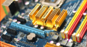
In electronics, there is the possibility that your PCB can get pretty hot due to power dissipation in certain components. There are many things to consider when dealing with heat in your board, and it starts with determining power dissipation in your design during schematic capture. If you happen to be operating within safe limits in a high power device, you might need an SMD heat sink on certain components. Ultimately, this could save your components, your product, and even the operator.

Read More
RF PCB
Blog • Sep 9, 2021
RF Power Supply Design and Layout Guide

One thing is certain: power supply designs can get much more complex than simply routing DC power lines to your components. RF power supply designs require special care to ensure they will function without transferring excessive noise between portions of the system, something that is made more difficult due to the high power levels involved. In addition to careful layout, circuitry needs to be designed such that the system provides highly efficient power conversion and delivery to each subsection of the system.

Read More
Prevent Overvoltage, Overcurrent and Heat logo
Blog • Sep 7, 2021
Methods to Protect your Circuit

Overvoltage, overcurrent, and heat are the three most likely events that can destroy our expensive silicon-based components or reduce our product’s life expectancy. The effects are often quite instant, but our product might survive several months of chronic overstress before giving up the ghost in some cases. Without adequate protection, our circuit can be vulnerable to damage, so what should we do? Or do we need to do anything?

Read More
SUBCKT sharing
Blog • Sep 2, 2021
SUBCKT Sharing: The Fastest Ways to Share SPICE Models Online

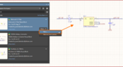
Today’s PCB designers and layout engineers often need to put on their simulation hat to learn more about the products they build. When you need to perform simulations, you need models for components, and simulation models often need to be shared with other team members at the project level or component level. What’s the best way for Altium Designer users to share this data? Read this article to learn more about sharing your models with other design participants. 

Read More
RF Printed Circuit Board
Blog • Aug 31, 2021
RF PCB Material Comparison for mmWave Devices

When some designers start talking materials, they probably default to FR4 laminates. The reality is there are many FR4 materials, each with relatively similar structure and a range of material property values. Designs on FR4 are quite different from those encountered at the low GHz range and mmWave frequencies. So what exactly changes at high frequencies, and what makes these materials different? To see just what makes a specific laminate useful as an RF PCB material, take a look at our guide below. 

Read More
Testing Challenges and Solutions
Blog • Aug 26, 2021
Low Cost Solutions for Automated Hardware in the Loop Testing

In today’s fast-paced world where iterations of electronics are spun at lightning speeds, we often forget one of the most critical aspects of development: testing. Even if we have that fancy test team, are we really able to utilize them for every modification, every small and insignificant change that we make to our prototypes? In this article, we will review a very low cost, yet highly effective and quite exhaustive test system that will get you that bang for your buck that you’ve been looking for.

Read More
  • Show More
Tag (field_common_tag)
Embedded thumbnail for Pi Filter Formulas and Simulation Deep Dive
How-To's • Dec 13, 2024
Pi Filter Formulas and Simulation Deep Dive

Learn the essentials of Pi filters, including how to size, design, and simulate them in Altium Designer. Host Zach Peterson explains the design equations for Pi filters, discusses online tools for accurate component selection, and demonstrates real-time simulations in Altium Designer to visualize the effects of impedance mismatches.

Start Watching
Embedded thumbnail for True Donut Pad Shapes
New in Altium Designer 25 • Dec 11, 2024
True Donut Pad Shapes

Check out our brand-new short video showcasing an exciting improvement in the PCB design process. Altium Designer 25 now supports true donut pad shapes, enhancing both your routing and performance.

Start Watching
Embedded thumbnail for Modernizing Engineering Workflows: Altium Designer 25 and the Future of Concurrent Design - Recording Preview
New in Altium Designer 25 • Dec 10, 2024
Modernizing Engineering Workflows: Altium Designer 25 and the Future of Concurrent Design - Recording Preview

Discover the new features in Altium Designer 25! This webinar recording highlights the Signal Analyzer by Keysight, advanced Wire Bonding capabilities, multi-board design enhancements, and more, showcasing how these tools can transform your PCB design process.

Start Watching
Embedded thumbnail for Dynamic Phase Matching and Tuning for Differential Pairs
New in Altium Designer 25 • Dec 5, 2024
Dynamic Phase Matching and Tuning for Differential Pairs

Explore how dynamic phase matching for differential pairs works with the improved match length rule in Altium Designer. Learn key techniques in this quick tutorial!

Start Watching
Embedded thumbnail for Obey Rules and Auto-Shrinking Features
New in Altium Designer 25 • Dec 4, 2024
Obey Rules and Auto-Shrinking Features

Discover how Altium Designer 25's Obey Rules and Auto-Shrinking features streamline routing, ensuring speed and precision while maintaining adherence to all design constraints.

Start Watching
Embedded thumbnail for Quickstart Guide: Single Layer PCB Design with Altium Designer 25
New in Altium Designer 25 • Nov 27, 2024
Quickstart Guide: Single Layer PCB Design with Altium Designer 25

Transform your designs with the new Single Layer PCB Design feature in Altium Designer 25! Whether you're working on Rigid-Flex projects or creating simple, space-saving boards, this tool makes the process faster, smarter, and more efficient. Watch our guide now and unlock your next big innovation.

Start Watching
Embedded thumbnail for How to Design Bending Regions in Flex PCBs
How-To's • Nov 25, 2024
How to Design Bending Regions in Flex PCBs

Watch our latest video on bending regions in flex PCBs! This step-by-step guide will show you how to configure stack-ups, distinguish between flex and rigid regions, and troubleshoot common issues in 3D views.

Start Watching
Embedded thumbnail for LDO Regulator Essentials: From Basics to Advanced. Part V: Ripple Rejection
LDO Regulator Essentials • Nov 22, 2024
LDO Regulator Essentials: From Basics to Advanced. Part V: Ripple Rejection

The final part of the LDO Regulator Essentials series focuses on voltage ripple rejection in Low Dropout Regulators (LDOs). Our host Rafał Stępień explains how LDOs clean up DC supply waves, ensuring stable performance in power systems. This episode provides practical insights for optimizing sensitive designs.

Start Watching
Embedded thumbnail for Explore Routing Improvements in Altium Designer 25
New in Altium Designer 25 • Nov 21, 2024
Explore Routing Improvements in Altium Designer 25

Discover Routing Improvements in Altium Designer 25. Learn about Dynamic Phase Matching, True Donut Pad Shape, and more in our latest video showcasing the powerful enhancements in our newest release.

Start Watching
Embedded thumbnail for Join our upcoming webinar and WIN Free Training!
New in Altium Designer 25 • Nov 19, 2024
Join our upcoming webinar and WIN Free Training!

Don't miss the chance to win FREE access to Mixed Simulation On-Demand Training! Be a part of our webinar on November 21 for our webinar, Modernizing Engineering Workflows: Altium Designer 25 and the Future of Concurrent Design. Register here: AD25 Webinar Registration Page. 

Start Watching
Embedded thumbnail for Wire Bonding Shorts: Die Footprints
New in Altium Designer 25 • Nov 18, 2024
Wire Bonding Shorts: Die Footprints

Check our new short video where Samer Aldhaher demonstrates the Wire Bonding feature in Altium Designer 25, including die-to-die and die-to-copper connections, multiple wire bonds, and pad rotation techniques.

Start Watching
Embedded thumbnail for Altium Designer 25: Collaboration at its Finest
New in Altium Designer 25 • Nov 13, 2024
Altium Designer 25: Collaboration at its Finest

Altium Designer 25 focuses on enhancing collaboration for engineering teams with new tools like the SI Analyzer by Keysight, updated PCB CoDesign, MCAD and Ansys CoDesigners, and improved Simulation modules. This release also introduces Wire Bonding, Single Layer PCB, and performance upgrades for optimized PCB design workflows. Check our overview video about all the improvements in this release.

Start Watching
Embedded thumbnail for The Fastest Ways to Run a PCB BOM Review
How-To's • Nov 12, 2024
The Fastest Ways to Run a PCB BOM Review

Conducting a BOM review is crucial to prevent costly delays, obsolete components, and unforeseen sourcing challenges in your PCB project. Discover powerful tools like DigiKey, Octopart, and Altium 365’s BOM portal to simplify your review process and ensure you're selecting the best parts at optimal prices.

Start Watching
Embedded thumbnail for Quantum Systems uses Altium Designer and Altium 365 to build the future of Drones
Altium Stories • Nov 6, 2024
Quantum Systems uses Altium Designer and Altium 365 to build the future of Drones

Quantum Systems creates advanced drones for critical aerial intelligence across industries. With Altium Designer and Altium 365, they streamline electronics engineering and enhance team collaboration. Watch how Altium software helps them innovate faster and build reliable drones for mission-critical moments.

Start Watching
Embedded thumbnail for Wire Bonding Shorts: 3D Stacked Die with Cavity
New in Altium Designer 25 • Nov 5, 2024
Wire Bonding Shorts: 3D Stacked Die with Cavity

Check our short video by Samer Aldhaher on using Altium Designer’s wire bonding tool for creating 3D stacked die in cavity. Highlights advanced techniques for compact, high-performance PCB designs with 3D integrated circuits.

Start Watching
Embedded thumbnail for Constraint Manager Improvements in Altium Designer 25
New in Altium Designer 25 • Nov 4, 2024
Constraint Manager Improvements in Altium Designer 25

Discover the latest in Altium Designer 25’s Constraint Manager, with updates like flexible net selection, streamlined rule management, and differential pair handling. Simplify your PCB design workflow with powerful new tools and enhancements.

Start Watching
  • Show More
Tag (field_common_tag)
ADv25
On-Demand Webinar • Oct 24, 2024
Modernizing Engineering Workflows: Altium Designer 25 and the Future of Concurrent Design
Struggling with team misalignment and design errors? Join our exciting webinar to discover the groundbreaking advancements in Altium Designer 25!
Watch Now
KiCad Webinar
On-Demand Webinar • Oct 16, 2024
Taking the Next Step: Growing Beyond KiCad with Altium
Join our upcoming webinar to discover how Altium Designer can transition your KiCad projects without any data loss
Watch Now
Synchronize to Optimize Jira Integration
On-Demand Webinar • Oct 7, 2024
Synchronize to Optimize: Enhancing Efficiency with Jira Integration for Altium 365
Tired of juggling multiple tools for project management? Watch the webinar and see how Jira Integration for Altium 365 can optimize your workflows.
Watch Now
Wire bonding
On-Demand Webinar • Sep 29, 2024
Unlock New Design Possibilities with Wire Bonding
Explore how wire bonding can enhance your designs, provide size reduction, improve power management, and increase mechanical reliability.
Watch Now
routing
On-Demand Webinar • Sep 29, 2024
Advanced Routing Features & Techniques
To help you get the most out of your experience with Altium Designer, join our webinar this month and learn advanced routing techniques.
Watch Now
signal analyzer
On-Demand Webinar • Sep 25, 2024
Signal Integrity Made Simple
Discover how to easily detect and resolve high-speed signal integrity challenges without the need for extensive expertise.
Watch Now
competitive-displacement-webinar-3
On-Demand Webinar • Sep 20, 2024
Mastering Design Complexity: How Altium Designer Outperforms Cadence in Solving Workflow and Engineering Challenges - Part 2
Join our webinar to learn how to enhance efficiency, foster better collaboration, and accelerate your time-to-market with Altium unified solutions.
Watch Now
Breaking Down Silos Webinar
On-Demand Webinar • Sep 16, 2024
Breaking Down Data Silos: A Practical Comparison of Altium and Cadence in Cross-Functional PCB Design
Join us for a webinar that addresses the critical challenges of maintaining design data continuity across various design functions.
Watch Now
Draftsman
On-Demand Webinar • Sep 10, 2024
Mastering Design Complexity: How Altium Designer Outperforms Cadence in Solving Workflow and Engineering Challenges
Join our upcoming webinar to discover why engineers consistently choose Altium Designer as the standard in PCB design.
Watch Now
SPICE
On-Demand Webinar • Sep 3, 2024
Mastering SPICE Simulation in Altium Designer
Discover how the SPICE engine in Altium Designer can help you easily verify that your finished project functions as intended.
Watch Now
Output job
On-Demand Webinar • Aug 24, 2024
Beyond PCB Design with Altium Designer
In this webinar we'll dive into the essential aspects that go beyond the schematic and layout.
Watch Now
PCB
On-Demand Webinar • Aug 23, 2024
Elevate Your Design Skills: Tips & Tricks for Success
Discover practical insights and efficient methods that can enhance your PCB design capabilities.
Watch Now
Cyber Security Webinar Cover
On-Demand Webinar • Aug 6, 2024
The Anatomy of IT Compliance in Electronics Development: Altium 365 & AWS GovCloud
Are you an IT or security professional looking for a secure electronics design collaboration platform that could also support your ITAR and EAR compliance efforts? If so, watch this webinar to bring together the expertise of Altium 365 and AWS!
Watch Now
Design reuse
On-Demand Webinar • Aug 1, 2024
How to Speed-up Product Development with Reusable Circuitry
In this webinar you'll learn more about the benefits of the design reuse blocks approach as well as the Design Reuse panel.
Watch Now
Harness design
On-Demand Webinar • Jul 19, 2024
Stay Ahead of the Curve: A Half-Year Review of Altium Designer Improvements
Join our exciting webinar to discover the groundbreaking advancements in Altium Designer!
Watch Now
Lenght Tuning
On-Demand Webinar • Jun 26, 2024
Achieve Precision and Speed with Altium Designer 24's Innovative Routing Features
Speed up your routing process and achieve better results for even your most demanding designs.
Watch Now
  • Show More
Tag (field_common_tag)
Loading
Loading...
Share link
Share with
Search by Update
Version
Update
25 26 24 23 22
25.0 25.1 25.2 25.3 25.4 25.5 25.6 25.7 25.8 25.9
26.1 26.2
24.10 24.9 24.8 24.7 24.6 24.5 24.4 24.3 24.2 24.1 24.0
23.11 23.10 23.9 23.8 23.7 23.6 23.5 23.4 23.3 23.2 23.1 23.0
22.11 22.10 22.9 22.8 22.7 22.6 22.5 22.4 22.3