
Main navigation

  • Home
  • Discover
  • Learning Center
  • What’s New

Second main navigation

  • Altium Community
  • Support
  • Documentation
×

Results

  • Updates
  • Blog 570
  • Video 539
  • Webinar 86
  • Playlist 53
Filters:
Tag (field_common_tag)
Blog • Oct 2, 2025
Most Common Causes of PCB Assembly Rework and Scrap

Many PCB assemblies fail not because of exotic faults, but due to basic issues like incorrect BOM entries or footprint mismatches that force rework or scrap. This article dives into the most common causes and how to prevent costly defects in your design-to-manufacturing process.

Read More
Embedded thumbnail for Mechanically Drilled Blind & Buried Vias: PCB Design Rules Explained
How-To's • Oct 1, 2025
Mechanically Drilled Blind & Buried Vias: PCB Design Rules Explained

Discover the essential design rules and manufacturing processes for mechanically drilled blind and buried vias in PCB layouts in this comprehensive tutorial. We cover the stack drill-and-plate fabrication process, aspect ratio limitations, sub-lamination design, and copper weight considerations. You’ll also learn how these vias differ from HDI microvias and gain a clear understanding of the critical design constraints needed for successful PCB manufacturing.

Start Watching
Blog • Sep 30, 2025
Behind the Scenes with AI Embedded Development

Forget one-shot AI hacks Ari Mahpour shows the thoughtful, sustainable way to integrate AI into embedded firmware development. Learn the core principles (planning gate, HAL abstraction, observability, timeout design) that can help you push your efficiency 5-10 times in real hardware projects.

Read More
Embedded thumbnail for Altium Training - Design Environment: Navigation with Schematic Workspace
Altium Training • Sep 29, 2025
Altium Training - Design Environment: Navigation with Schematic Workspace

Discover the most important navigation techniques for the schematic workspace using both mouse and keyboard controls. In this tutorial video, you’ll learn how to use the View menu commands for document fitting, area zooming, and object selection, along with advanced navigation shortcuts. Master mouse-based panning and zooming, explore Ctrl key combinations, and practice arrow key movements - all designed to simplify your workflow in the PCB design process.

Start Watching
Blog • Sep 25, 2025
We're heading to PCB West 2025!

Join Altium at PCB West 2025 in Santa Clara, CA, on October 1! Stop by Booth 300 for the official launch of the new Altium platform, built on the foundation of Altium Designer and Altium 365. Be sure to check out our live demos of Altium Develop and Altium Agile.

Read More
Blog • Sep 24, 2025
Peak Electrical Performance in Multi-Board Designs With Advanced Simulation and Compliance Tools

Moving from single-board to multi-board systems is a leap in complexity. You must manage not just routing, but power, signal integrity, mechanical fit, and regulatory requirements across boards. In this article, you’ll discover how Altium’s advanced simulation and compliance tools help engineering teams overcome these challenges and deliver reliable multi-board solutions.

Read More
Embedded thumbnail for Altium Training - Design Environment: The Altium Environment
How-To's • Sep 23, 2025
Altium Training - Design Environment: The Altium Environment

Get familiar with the core workspace layout and navigation methods. In this video, you’ll see how to open schematic and PCB documents, work within the unified design environment, and move between multiple open files using document tabs and keyboard shortcuts.

Start Watching
Blog • Sep 22, 2025
How to Catch Enclosure and Connector Misalignment Before the First Prototype

As electronics continue to miniaturize and functionality increases, even minor misalignments between enclosures and connectors can derail a project. This article explores how early integration of ECAD and MCAD workflows helps detect and eliminate those costly issues before the first prototype is built.

Read More
Embedded thumbnail for Altium Training - Design Environment: Opening a Project from a Local Drive
Altium Training • Sep 18, 2025
Altium Training - Design Environment: Opening a Project from a Local Drive

Get your PCB design workflow off to a smooth start. This Altium tutorial walks you through opening projects from your local directory - a core skill that keeps your process efficient and organized from day one.

Start Watching
Blog • Sep 17, 2025
Executive Insights Into Electronic Product Development Gaps You Need To Close

Electronics hardware development is falling behind broader product development disciplines due to fragmented workflows, poor collaboration, and limited compliance visibility. This gap introduces risk, delays, and missed opportunities but executives see real business value in modernizing electronics development through better integration, traceability, and lifecycle visibility.

Read More
Embedded thumbnail for Altium Essentials: Design Environment
Altium Training • Sep 16, 2025
Altium Essentials: Design Environment

Take control of your PCB design workflow with Altium Essentials: Design Environment. This tutorial module guides you through the fundamentals of workspace management, from handling panels and documents to mastering menus, context commands, and time-saving shortcuts.

Start Watching
Blog • Sep 15, 2025
Sourcing For High-Mix Low-Volume Electronics Manufacturing

High-mix, low-volume (HMLV) electronics manufacturing requires agile sourcing strategies to handle shifting BOMs, erratic lead times, and component volatility. All while controlling costs and ensuring compliance. Cloud-based tools like Altium provide real-time component visibility, BOM collaboration, and supplier integrations to help navigate HMLV complexities.

Read More
Embedded thumbnail for What Makes a Great PCB Design Review Submission?
How-To's • Sep 11, 2025
What Makes a Great PCB Design Review Submission?

Turn your PCB designs into professional-grade submissions. At Altium, we reveal the key practices that transform schematics, layouts, and documentation into review-ready work that stands out. Watch our brand-new tutorial and take your PCB design process to the next level.

Start Watching
Blog • Sep 10, 2025
How to Solve Fit, Form, and Function Challenges in Robotics with ECAD-MCAD Collaboration

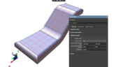
As robotics systems become increasingly miniaturized and intricate, ensuring perfect fit, form, and function across electrical and mechanical domains is critical to avoid design setbacks. Real-time ECAD-MCAD integration with two-way sync empowers teams to streamline workflows, reduce PCB rework, and deliver more reliable designs faster.

Read More
Embedded thumbnail for Altium Training - Workspace Folder Structure: Opening the Explorer Panel
Altium Training • Sep 9, 2025
Altium Training - Workspace Folder Structure: Opening the Explorer Panel

Discover the key ways to access the Explorer panel in Altium Designer with this step-by-step tutorial. The video walks you through four different methods, giving you the freedom to choose the approach that best fits your workflow.

Start Watching
Blog • Sep 8, 2025
One Vision, Three Powerful Solutions: Introducing Altium Discover, Altium Develop, and Altium Agile

We are excited to announce the launch of three new platform-based solutions that will transform the way electronic products are designed, built, and delivered: Altium Discover, Altium Develop, and Altium Agile. These solutions are designed to simplify processes, accelerate innovation, and make collaboration seamless across the entire electronics lifecycle. Together, they realize the purpose of Altium and Renesas: To Make Our Lives Easier.

Read More
  • Show More
Tag (field_common_tag)
Altium 365 SOC 2 Type 1 Certified
Blog • Feb 15, 2022
Announcing SOC 2 Type 1 Certification for Altium 365

We are pleased to announce that Altium 365 is officially SOC 2 Type 1 certified. System and Organization Controls (SOC) 2 is a widely recognized attestation of security compliance defined by the AICPA and is considered the standard for ensuring data security and operational maturity. A SOC 2 certification provides valuable information for companies to assess the quality of the security provided by a service such as Altium 365.

Read More
Three ways to manage your BOM costs
Blog • Feb 10, 2022
Improving Supply Chain Success with BOM Management

It’s no secret that component shortages have become more frequent this year. Companies will continue to grapple with supply chain challenges into 2022 and beyond. The impact of manufacturing delays can be substantial if a part is not available. Delays occur and sales plans get put on hold. It can also be very expensive and risky to replace parts from multiple sources. Fortunately, many shortages can be avoided by introducing proactive supply chain practices.

Read More
Reliability and failure analysis
Blog • Feb 8, 2022
Overview of PCB/PCBA Reliability and Failure Analysis

Reliability testing and failure analysis of a PCB/PCBA go hand-in-hand; when designs are stressed to the limit, their failure modes need to be determined through thorough inspection and analysis. To get started on this topic, it’s important to understand the qualification aspects that will govern your bare board design and the PCBA. We’ll look at the various dimensions of PCB/PCBA reliability, as well as some of the standard failure analysis techniques used to identify potential design change requirements.

Read More
Plane and Cavity Resonances
Blog • Feb 3, 2022
When Do PCB Power Plane Resonances Occur?

By now, designers should be aware of some important behavior involved in power delivery to components in a PCB, particularly for digital components. All digital components produce and manipulate wideband signals, where the frequency content theoretically extends up to infinite frequency. As such, some radiation may propagate through your PCB, leading to resonant behavior that is not observed on the power rail.

Read More
Selecting a plating material
Blog • Feb 1, 2022
How to Choose PCB Plating for Your Finished Board

Once your board passes through the standard PCB fabrication process, the bare copper in your PCB will be ready for the application of a surface finish. PCB plating is applied to protect any copper in your PCB that would be exposed through the solder mask, whether it’s a pad, via, or other conductive element. In this article, I’ll run over the different PCB plating material options and their advantages in your PCB. 

Read More
What is the PCB Supply Chain?
Blog • Jan 27, 2022
What is the PCB Supply Chain?

The PCB supply chain encompasses multiple components, raw materials, and the PCB itself. PCBs and PCB assemblies are often the most technically complex components that are purchased for electronic assemblies and products. The complexity of modern PCBs leads to several challenges for a supply chain management team that may be significantly different when compared with other commodities the team manages. In this brief guide, we'll look in-depth at the PCB supply chain, and specifically what falls within the purview of a procurement and supply chain management team.

Read More
What is mode conversion
Blog • Jan 25, 2022
A Guide to Mode Conversion, Its Causes, and Solutions

On interconnects, such as board-to-board connections or cascaded transmission line arrangements, you have an important EMC compliance metric that is sometimes overlooked. This is mode conversion, which can be visualized in an S-parameter measurement for differential and common-mode signal transmission. In this article, we’ll look at a short overview of mode conversion in high-speed design with some examples from common differential standards.

Read More
Pad and via sizing
Blog • Jan 20, 2022
PCB Via Size and Pad Size Guidelines

There are some aspects of PCB design and layout that seem deceptively simple, and yet they have a complex answer that is related to many important aspects of manufacturing. One of these design aspects is the match between PCB via size and pad size. Obviously, these two points are related; all vias have a landing pad that supports the via and provides a place to route traces into a via pad. However, there are some important sizing guidelines to follow when the matching pad and via sizes, and this match is an important element of DFM and reliability.

Read More
Differential Microstrip Impedance
Blog • Jan 18, 2022
Differential Microstrip Impedance Calculator

Are you looking for a free tool that you can use to calculate the impedance of differential microstrips? We created a simple tool you can use to calculate differential microstrip impedance for a given geometry and dielectric constant. If you’ve been looking for an accurate differential microstrip impedance calculator, then the calculator below is certainly one of the best free tools you’ll find on the internet before you start using field solvers to determine differential pair impedance.

Read More
PCB DFM Check
Blog • Jan 13, 2022
Getting Through a PCB DFM Check

In this article, we’ll discuss the key design features to implement, and steps to take prior to fabrication that will help prevent some common DFM problems. I’ll also provide examples of where I commonly see these PCB DFM problems in signal integrity circuits.

Read More
Spreading Inductance
Blog • Jan 11, 2022
What is Spreading Inductance?

If you’re working with a high-speed digital component, there are some simple power integrity rules that should be followed. However, there is one quantity that is sometimes ignored when building a PDN impedance simulation: the spreading inductance of your plane pair. Here are some points designers should know about the spreading inductance of a plane pair.

Read More
PCB Design Basics for New Designers
Blog • Jan 6, 2022
PCB Design Basics for New Designers

In this article, I’ll present some design basics that every new designer should follow to help ensure their design process is successful. Some of these points may challenge the conventional view of how circuit boards are constructed, but they are intended to help balance low noise signaling, manufacturability, and ease of solving a layout.

Read More
Selecting Materials for High Voltage PCB Design and Layout
Blog • Jan 4, 2022
Selecting Materials for High Voltage PCB Design and Layout

High voltage PCBs are subject to certain safety and reliability concerns that you won’t find in most other boards. If your fabrication house specializes in high voltage PCBs and keeps materials in stock, they can likely recommend a material set, as well as a standard stackup you might use for certain voltage ranges and frequencies. If you need to choose your own materials, follow the tips below to help you narrow down to the right material set.

Read More
Via tenting in PCB Layout
Blog • Dec 28, 2021
When to Use Tented Vias in Your PCB Layout

There are some guidelines I see many designers implement as a standard practice, often without thinking about it. Some of these practices are misunderstood or implemented without best practices. Others are implemented without thinking about the potential problems. One of these is the use of tented vias, which is sometimes implemented in a PCB layout by default. Is this always the right practice?

Read More
Capacitive load termination
Blog • Dec 23, 2021
How to Impedance Match and Terminate Capacitive Loads

The idea of a purely capacitive load is something of a fallacy. Yes, capacitors exist, but all capacitors are non-ideal, and it is this deviation from a theoretical capacitance that determines how to impedance match a load that exhibits capacitive behavior. Let’s take a look at this important aspect of interconnect design and see what it really means to terminate a capacitive load.

Read More
Using Altium 365 Over Your Vanilla Version Control System
Blog • Dec 20, 2021
Using Altium 365 Over Your Vanilla Version Control System

There are all sorts of version control systems out there that people have been using with their PCB design software. As discussed in Why Use a Version Control System, we looked at different options ranging for local hard drive storage to sophisticated online revisioning systems. In this article we will be reviewing the differences between a standard VCS and Altium 365.

Read More
  • Show More
Tag (field_common_tag)
Embedded thumbnail for Auto-tuning Your Way to Faster PCB Design
Altium Designer's 25 Quantitative Benefits • Jun 13, 2025
Auto-tuning Your Way to Faster PCB Design

Watch how the Auto Tuning feature in Altium Designer 25 delivers optimized DDR4 routing in a single click! Fewer steps, massive time savings. Try our Benefit Calculator to estimate your own time and cost savings.

Start Watching
Embedded thumbnail for Enhanced Constraint Manager in Altium Designer 25. Part I: From Directives to Creepage Rules
Enhanced Constraint Manager in Altium Designer 25 • Jun 9, 2025
Enhanced Constraint Manager in Altium Designer 25. Part I: From Directives to Creepage Rules

We are introducing a new video series on the Enhanced Constraint Manager in Altium Designer 25. In the first chapter, Samer Aldhaher demonstrates how to define net classes, apply clearance and creepage rules, and validate constraints within both the schematic and PCB. The video uses a 1kW, 400V brushless DC motor driver project to illustrate real-world applications.

Start Watching
Embedded thumbnail for Design Faster with Altium Designer 25
Altium Designer's 25 Quantitative Benefits • Jun 6, 2025
Design Faster with Altium Designer 25

Every second and every click count in the product development cycle. See how the new PCB Layout Replication feature in Altium Designer 25 boosts your efficiency in the PCB design process. Want to improve even more? Check out our Benefit Calculator now!

Start Watching
Embedded thumbnail for Creating PCB Drill Drawings and Tables in Altium Designer
How-To's • Jun 5, 2025
Creating PCB Drill Drawings and Tables in Altium Designer

If you want to learn more about drill drawings and tables in your PCB designs using Altium Designer, this tutorial is a must-watch. In the video, our Tech Consultant Zach Peterson walks you through multiple methods for generating these critical fabrication documents, including automatic Gerber outputs and custom drawings.

Start Watching
Embedded thumbnail for Streamlining Team Collaboration in Industrial PCB Projects - Recording Preview
New in Altium Designer 25 • Jun 4, 2025
Streamlining Team Collaboration in Industrial PCB Projects - Recording Preview

This webinar recording shows how Altium Designer and Altium 365 improve team collaboration in industrial PCB projects. It covers features like version control, live commenting, task tracking, and JIRA integration to help teams work more efficiently and reduce costly errors.

Start Watching
Embedded thumbnail for AC Coupling Capacitors: Placement for High-Speed PCB Design
How-To's • May 28, 2025
AC Coupling Capacitors: Placement for High-Speed PCB Design

Learn the facts about AC coupling capacitor placement in high-speed PCB designs. In this video, Zach Peterson explores the ongoing debate: should AC coupling capacitors be placed near the transmitter or the receiver in high-speed differential pairs?

Start Watching
Embedded thumbnail for Coming Soon: Export 3D-MID Tracks as Centerline Curves
New in Altium Designer 25 • May 23, 2025
Coming Soon: Export 3D-MID Tracks as Centerline Curves

Coming Soon: 3D-MID Track-to-Centerline Export allows you to export conductive tracks on 3D substrates as precise centerline curves within STEP files—enabling seamless integration with advanced 5-axis manufacturing processes. Explore more upcoming upgrades on our Coming Soon page.

Start Watching
Embedded thumbnail for Advanced xSignal and Impedance Control Techniques - Recording Preview
New in Altium Designer 25 • May 20, 2025
Advanced xSignal and Impedance Control Techniques - Recording Preview

This webinar recording explores advanced xSignal and impedance control techniques in Altium Designer 25. It covers defining xSignals, managing impedance profiles, differential pairs, and delay tuning—all essential for high-speed PCB design. Full recording you find here: April 2025 COM Webinar Recording.

Start Watching
Embedded thumbnail for Coming Soon: Embedded 3D Models for Harness Designs
How-To's • May 16, 2025
Coming Soon: Embedded 3D Models for Harness Designs

Coming soon: the Embedded 3D Models for Harness Designs feature will automatically include Parasolid-format 3D models in your harness layout drawings. This improves integration with MCAD CoDesigner, enabling seamless synchronization between electrical and mechanical design domains. To see more upcoming upgrades, visit our Coming Soon page.

Start Watching
Embedded thumbnail for Make Smarter Design Decisions with Signal Analyzer by Keysight
New in Altium Designer 25 • May 14, 2025
Make Smarter Design Decisions with Signal Analyzer by Keysight

Discover how to simplify your workflow and boost design confidence with Signal Analyzer by Keysight—a complete extension available right inside Altium Designer 25. This whitepaper shows you how to analyze impedance, delay, and insertion/return loss without ever leaving your design environment.

Start Watching
Embedded thumbnail for Unveiling 86% Task Time Efficiency in Altium Designer 25
Altium Designer's 25 Quantitative Benefits • May 9, 2025
Unveiling 86% Task Time Efficiency in Altium Designer 25

Watch how Altium Designer 25 saves time on PCB visualization. This short video shows a side-by-side comparison of the same task done in Altium Designer 25 vs. an external CAD tool—revealing big time and click savings. A great teaser to highlight the value of the unified design environment and promote the Benefit Calculator.

Start Watching
Embedded thumbnail for AGND vs PGND: Proper Net Tie Connections in Power Regulator PCB Design
How-To's • May 8, 2025
AGND vs PGND: Proper Net Tie Connections in Power Regulator PCB Design

What’s the difference between AGND and PGND — and when should you use a net tie? Zach Peterson breaks down proper PCB layout for buck converters, grounding best practices, and why component placement matters in switching regulator designs.

Start Watching
Embedded thumbnail for  Students at Monash UAS Fly Higher with Altium Solutions to Power Their Autonomous Drone Technology
Altium Stories • May 2, 2025
Students at Monash UAS Fly Higher with Altium Solutions to Power Their Autonomous Drone Technology

Discover how the Monash Uncrewed Aerial Systems team leverages Altium Designer, MCAD CoDesigner, and Altium 365 to develop custom drone boards for critical humanitarian missions.

Start Watching
Embedded thumbnail for Say Goodbye to Disjointed Workflows: Unified Product Design in Altium Designer 25
New in Altium Designer 25 • Apr 29, 2025
Say Goodbye to Disjointed Workflows: Unified Product Design in Altium Designer 25

Check an overview of how Altium Designer 25 unifies Multi-Board and Harness Design into a seamless, efficient workflow for faster, error-free product development.

Start Watching
Embedded thumbnail for From Concept to Reality: Updated 3D-MID Demo in Altium Designer 25
New in Altium Designer 25 • Apr 28, 2025
From Concept to Reality: Updated 3D-MID Demo in Altium Designer 25

A walkthrough of the new 3D-MID capabilities in Altium Designer 25. Covers setting up a 3D PCB document, component placement on curved surfaces, routing with grids and sketches, exporting for LDS manufacturing, and generating a 3D pick-and-place file.

Start Watching
Embedded thumbnail for Take 66% of Your Time Back with Custom Pad Stack in Altium Designer 25
Altium Designer's 25 Quantitative Benefits • Apr 24, 2025
Take 66% of Your Time Back with Custom Pad Stack in Altium Designer 25

This video demonstrates the measurable productivity gains of using the Custom Pad Stack tool in Altium Designer 25. It compares a detailed QFN-32 footprint customization process across versions, showing a significant reduction in time and mouse clicks—2 min 5 sec vs. 6 min 2 sec, and 45 vs. 116 clicks.

Start Watching
  • Show More
Tag (field_common_tag)
 Preventing Obsolescence Before It Hits
On-Demand Webinar • Jun 12, 2025
Proactive Lifecycle Management: Preventing Obsolescence Before It Hits
Take the first step toward eliminating avoidable delays and costly redesigns. Don't miss it and register now!
Watch Now
Integrating Requirements June 2025 Webinar
On-Demand Webinar • May 28, 2025
Integrating Requirements into Your PCB Design Workflow
Join our webinar where you will learn about integrated requirements tools who can help you eliminate late-stage design changes, AI support through system requirements and integration of design requirements directly in PCB Design. Don't miss it, register now!
Watch Now
A365 Webinar
On-Demand Webinar • Apr 23, 2025
Collaborative Design Review: Ensuring Quality from Schematics to Supply Chain
Join our live webinar to learn how Altium 365 accelerates collaboration, standardizes workflows, and ensures design integrity to mitigate risks and accelerate time to market.
Watch Now
Webinar: From Prototype to Production: Optimizing BOM Costs Without Compromising Quality with Part Analytics
On-Demand Webinar • Apr 22, 2025
From Prototype to Production: Optimizing BOM Costs Without Compromising Quality with Part Analytics
Learn how to reduce production BOM costs without redesign, explore techniques to consolidate part demand for volume savings, and discover case examples from supply chain teams that increased sourcing process efficiency by up to 97%.
Watch Now
Streamlining Team Collaboration
On-Demand Webinar • Apr 17, 2025
Streamlining Team Collaboration in Industrial PCB Projects
Join us for our upcoming webinar to discover how Altium Designer and Altium 365 can transform your team’s collaboration and take your PCB design projects to the next level. Attend for a chance to win free access to the Altium 365 Training Bundle.
Watch Now
Component management
On-Demand Webinar • Apr 10, 2025
Ensure Best Designs with Professional Library Management
In this webinar, you'll discover how Altium Designer facilitates robust component management, including adding part choices to mitigate supply chain risks and leveraging Altium 365 managed components.
Watch Now
April 2025 Webinar Cover
On-Demand Webinar • Apr 9, 2025
Component Selection in Altium Designer: Making Data-Driven Decisions with Data Integrations
Improve component selection with real-time data insights in Altium 365! Join our live webinar to optimize your PCB development. Sign up now!
Watch Now
Altium Agile
Live Webinar
Altium Agile Teams - Sneak Peek
Get a first glimpse into this new Electronic Product Development Platform.
Jan
21
English
3:00 PM, CET
Jan
21
German
10:00 AM, CET
Jan
22
Italian
10:00 AM, CET
Jan
22
French
3:00 PM, CET
Jan
22
Spanish
3:00 PM, CET
Register Now
Altium Designer Overview
On-Demand Webinar • Dec 4, 2025
Altium Designer Onboarding Workshop
Join our live training workshop and see Altium Designer in action—from creating your first schematic to delivering ready-to-manufacture PCB files.
Watch Now
Altium Platform
On-Demand Webinar • Nov 21, 2025
Altium Platform - A foundation to meet your & your company’s targets
Discover how the Altium platform makes multidisciplinary cooperation easy and efficient.
Watch Now
Harness design
On-Demand Webinar • Nov 17, 2025
From single PCB to Harnessed Product
Discover how to streamline PCB-to-harness design with Altium’s powerful tools and boost collaboration across disciplines.
Watch Now
3D-MID Design
On-Demand Webinar • Oct 20, 2025
3D-MID Design in Altium
Discover how even complex products for 3D circuit designs are implemented easily in Altium.
Watch Now
Altium Designer Overview
On-Demand Webinar • Aug 20, 2025
Altium Designer and Altium 365 Overview
In this webinar we will show you how easy it is to create a prototype from scratch using Altium Designer in combination with Altium 365.
Watch Now
Altium Enterprise
On-Demand Webinar • Aug 3, 2025
Safety & Reliability in Electronics Design – Strategies, Standards & Tools
How can development teams and decision-makers effectively implement safety, security, and compliance without delaying innovation?
Watch Now
Altium Enterprise
On-Demand Webinar • Aug 2, 2025
Sustainability & Energy Efficiency in Electronic Product Development
Watch Now
Proactive Component Selection
On-Demand Webinar • May 22, 2025
Proactive Component Selection: Mitigating Manufacturing Delays Before They Happen
Most teams spend hours on component research yet still face redesigns. Learn how Altium 365 helps you make proactive, data-driven part decisions. Join SiliconExpert’s Jackie Sartin to discover smarter sourcing with real-time insights and validated alternatives.
Watch Now
  • Show More
Tag (field_common_tag)
Loading
Loading...
Share link
Share with
Search by Update
Version
Update
25 26 24 23 22
25.0 25.1 25.2 25.3 25.4 25.5 25.6 25.7 25.8 25.9
26.1 26.2
24.10 24.9 24.8 24.7 24.6 24.5 24.4 24.3 24.2 24.1 24.0
23.11 23.10 23.9 23.8 23.7 23.6 23.5 23.4 23.3 23.2 23.1 23.0
22.11 22.10 22.9 22.8 22.7 22.6 22.5 22.4 22.3