
Main navigation

  • Home
  • Discover
  • Learning Center
  • What’s New

Second main navigation

  • Altium Community
  • Support
  • Documentation
×

Results

  • Updates
  • Blog 570
  • Video 540
  • Webinar 86
  • Playlist 53
Filters:
Tag (field_common_tag)
Embedded thumbnail for Altium Training - Design Environment: Documents and Panels
Altium Training • Oct 6, 2025
Altium Training - Design Environment: Documents and Panels

In our new tutorial, we explore different panel display modes, including docked, floating, and tabbed grouping arrangements. Effective panel management is essential for creating an efficient design environment tailored to your specific workflow requirements.

Start Watching
Blog • Oct 2, 2025
Most Common Causes of PCB Assembly Rework and Scrap

Many PCB assemblies fail not because of exotic faults, but due to basic issues like incorrect BOM entries or footprint mismatches that force rework or scrap. This article dives into the most common causes and how to prevent costly defects in your design-to-manufacturing process.

Read More
Embedded thumbnail for Mechanically Drilled Blind & Buried Vias: PCB Design Rules Explained
How-To's • Oct 1, 2025
Mechanically Drilled Blind & Buried Vias: PCB Design Rules Explained

Discover the essential design rules and manufacturing processes for mechanically drilled blind and buried vias in PCB layouts in this comprehensive tutorial. We cover the stack drill-and-plate fabrication process, aspect ratio limitations, sub-lamination design, and copper weight considerations. You’ll also learn how these vias differ from HDI microvias and gain a clear understanding of the critical design constraints needed for successful PCB manufacturing.

Start Watching
Blog • Sep 30, 2025
Behind the Scenes with AI Embedded Development

Forget one-shot AI hacks Ari Mahpour shows the thoughtful, sustainable way to integrate AI into embedded firmware development. Learn the core principles (planning gate, HAL abstraction, observability, timeout design) that can help you push your efficiency 5-10 times in real hardware projects.

Read More
Embedded thumbnail for Altium Training - Design Environment: Navigation with Schematic Workspace
Altium Training • Sep 29, 2025
Altium Training - Design Environment: Navigation with Schematic Workspace

Discover the most important navigation techniques for the schematic workspace using both mouse and keyboard controls. In this tutorial video, you’ll learn how to use the View menu commands for document fitting, area zooming, and object selection, along with advanced navigation shortcuts. Master mouse-based panning and zooming, explore Ctrl key combinations, and practice arrow key movements - all designed to simplify your workflow in the PCB design process.

Start Watching
Blog • Sep 25, 2025
We're heading to PCB West 2025!

Join Altium at PCB West 2025 in Santa Clara, CA, on October 1! Stop by Booth 300 for the official launch of the new Altium platform, built on the foundation of Altium Designer and Altium 365. Be sure to check out our live demos of Altium Develop and Altium Agile.

Read More
Blog • Sep 24, 2025
Peak Electrical Performance in Multi-Board Designs With Advanced Simulation and Compliance Tools

Moving from single-board to multi-board systems is a leap in complexity. You must manage not just routing, but power, signal integrity, mechanical fit, and regulatory requirements across boards. In this article, you’ll discover how Altium’s advanced simulation and compliance tools help engineering teams overcome these challenges and deliver reliable multi-board solutions.

Read More
Embedded thumbnail for Altium Training - Design Environment: The Altium Environment
How-To's • Sep 23, 2025
Altium Training - Design Environment: The Altium Environment

Get familiar with the core workspace layout and navigation methods. In this video, you’ll see how to open schematic and PCB documents, work within the unified design environment, and move between multiple open files using document tabs and keyboard shortcuts.

Start Watching
Blog • Sep 22, 2025
How to Catch Enclosure and Connector Misalignment Before the First Prototype

As electronics continue to miniaturize and functionality increases, even minor misalignments between enclosures and connectors can derail a project. This article explores how early integration of ECAD and MCAD workflows helps detect and eliminate those costly issues before the first prototype is built.

Read More
Embedded thumbnail for Altium Training - Design Environment: Opening a Project from a Local Drive
Altium Training • Sep 18, 2025
Altium Training - Design Environment: Opening a Project from a Local Drive

Get your PCB design workflow off to a smooth start. This Altium tutorial walks you through opening projects from your local directory - a core skill that keeps your process efficient and organized from day one.

Start Watching
Blog • Sep 17, 2025
Executive Insights Into Electronic Product Development Gaps You Need To Close

Electronics hardware development is falling behind broader product development disciplines due to fragmented workflows, poor collaboration, and limited compliance visibility. This gap introduces risk, delays, and missed opportunities but executives see real business value in modernizing electronics development through better integration, traceability, and lifecycle visibility.

Read More
Embedded thumbnail for Altium Essentials: Design Environment
Altium Training • Sep 16, 2025
Altium Essentials: Design Environment

Take control of your PCB design workflow with Altium Essentials: Design Environment. This tutorial module guides you through the fundamentals of workspace management, from handling panels and documents to mastering menus, context commands, and time-saving shortcuts.

Start Watching
Blog • Sep 15, 2025
Sourcing For High-Mix Low-Volume Electronics Manufacturing

High-mix, low-volume (HMLV) electronics manufacturing requires agile sourcing strategies to handle shifting BOMs, erratic lead times, and component volatility. All while controlling costs and ensuring compliance. Cloud-based tools like Altium provide real-time component visibility, BOM collaboration, and supplier integrations to help navigate HMLV complexities.

Read More
Embedded thumbnail for What Makes a Great PCB Design Review Submission?
How-To's • Sep 11, 2025
What Makes a Great PCB Design Review Submission?

Turn your PCB designs into professional-grade submissions. At Altium, we reveal the key practices that transform schematics, layouts, and documentation into review-ready work that stands out. Watch our brand-new tutorial and take your PCB design process to the next level.

Start Watching
Blog • Sep 10, 2025
How to Solve Fit, Form, and Function Challenges in Robotics with ECAD-MCAD Collaboration

As robotics systems become increasingly miniaturized and intricate, ensuring perfect fit, form, and function across electrical and mechanical domains is critical to avoid design setbacks. Real-time ECAD-MCAD integration with two-way sync empowers teams to streamline workflows, reduce PCB rework, and deliver more reliable designs faster.

Read More
Embedded thumbnail for Altium Training - Workspace Folder Structure: Opening the Explorer Panel
Altium Training • Sep 9, 2025
Altium Training - Workspace Folder Structure: Opening the Explorer Panel

Discover the key ways to access the Explorer panel in Altium Designer with this step-by-step tutorial. The video walks you through four different methods, giving you the freedom to choose the approach that best fits your workflow.

Start Watching
  • Show More
Tag (field_common_tag)
Blog • Dec 20, 2023
Design Phase – Lid Assembly Electronics Part 1

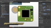
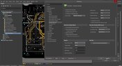
We are advancing our Open Source Laptop project to the next stage: assembling lid electronics. In the first part of this phase, we are focusing on the electronics and PCB design of the webcam module.

Read More
Common Challenges Stopping Your Production Line Cover Photo
Blog • Dec 19, 2023
3 Common Challenges Stopping Your Production Line

The efficiency of production lines is crucial for any successful hardware product development. However, some challenges derail these processes. Do you face these problems, too? Let’s find out!

Read More
Blog • Dec 15, 2023
Explore New Possibilities with True 3D-MID Design

3D-MID technology seamlessly integrates electrical circuits with three-dimensional mechanical parts. This unique fusion of functionality unlocks a myriad of possibilities across various application areas. Explore more about this innovative feature, available in Altium Designer 24, to delve into the fascinating world of the 3D design process.

Read More
Blog • Dec 13, 2023
Strategies to Minimize PCB Damage

The PCB design process is always an exciting journey for a designer or the founder of a project. The first run of it can be breathtaking. In this article, we delve into strategies for minimizing PCB damage in the case of an exemplary circuit.

Read More
Fragmented Feedback Loops Cover Photo
Blog • Dec 12, 2023
Fragmented Feedback Loops: The Hidden Cost in PCB Design and Testing

Explore the hidden impact of fragmented feedback loops in PCB design and testing. Check how minor communication gaps lead to significant financial burdens and learn how to address them.

Read More
GovCloud 101 Cover Photo
Blog • Dec 8, 2023
Altium 365 GovCloud 101: Everything You Need to Know

Would you like to improve the protection of your data? Altium 365 GovCloud can help you achieve these goals. It’s a version of Altium 365, engineered to meet the stringent demands of US government regulations.

Read More
Blog • Dec 4, 2023
Design Phase – Lid Assembly Mechanics Part 3

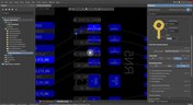
We are heightening the anticipation for our Open Source Laptop project. In this chapter, we delve into the ambient light sensor module. Learn more about how to implement it into this project.

Read More
Blog • Nov 30, 2023
PCB CoDesign: Design Faster Together

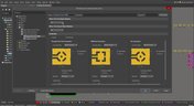
Experience accelerated design collaboration with PCB CoDesign, exclusively available on Altium Designer starting from December 13th. This innovative feature adopts a collaborative approach by seamlessly integrating schematic and PCB design, enabling multiple engineers to work on the same project. Explore this cutting-edge feature on our newly launched page dedicated to its functionalities.

Read More
Accelerate the Development of Complex Products Cover Photo
Blog • Nov 28, 2023
6 Steps to Accelerate the Development of Complex Products

Learn the key lessons from the presentation at Iteration22; “Joe Justice, Wikispeed - Everyone Must Be a Chief Engineer at SpaceX.” Read on and discover how to speed up the development of complex products. 

Read More
Blog • Nov 27, 2023
Design Phase – Lid Assembly Mechanics Part 2

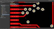
We are continuing our journey into lid assembly mechanics inside the Open Source Laptop Project. In this chapter, we are focusing on the sensor PCB above the display panel.

Read More
Assembly Assistant Blog Cover
Blog • Nov 21, 2023
How to Speed Up Your Manual Assembly Process with Assembly Assistant? The Story of XVP Photonics

Are you struggling with your manual assembly process? Would you like to speed it up and improve component placement accuracy? Read the story of XVP Photonics; with Assembly Assistant, they improved the component placement time by 25%. Discover how!

Read More
Blog • Nov 20, 2023
45V-5A Adjustable Half-Bridge DC to DC Converter

DC-to-DC buck converters are extensively employed in electronic devices. In this article, we will introduce you to one of our new projects—a DC-to-DC converter designed to serve as a power supply as well.

Read More
The Challenges of Modern Design Cover Photo
Blog • Nov 15, 2023
The Challenges of Modern Design: Why Requirements Management Is Essential

You need a robust requirements management process to ensure your design intent communication stays clear and organized. Read on to explore the crucial connection between well-managed requirements and today’s design.

Read More
Blog • Nov 14, 2023
Efficiency And Noise Top 10 Switching Regulator Modules

Switching regulator modules have become indispensable in a wide array of electronic devices, providing a more efficient means of voltage conversion between different levels by storing and releasing energy. Explore further insights into these devices in today's dynamic world of electronics.

Read More
Blog • Nov 10, 2023
Add USB Type-C Power Delivery to Your Designs!

We want to invite you to explore the fundamentals of USB Type-C Power Delivery which is now the most popular energy transmission in current times. We will show you how to easily incorporate a dedicated PD IC into your own designs. 

Read More
Blog • Nov 8, 2023
Design Phase – Lid Assembly Mechanics Part 1

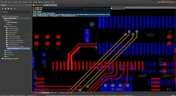
It is time to delve deep into the mechanical design of our Open Source Laptop project. In this article we give you an update about the first part of fitting elements into the system. You will learn more about laptop lid, webcam integration, light sensor and microphones which will be used in this project.

Read More
  • Show More
Tag (field_common_tag)
Embedded thumbnail for Searching for Errors
• Jun 16, 2020
Searching for Errors

We’ve looked at how to set up the Design Rule Checker to help us analyze our PCB design errors. Now it’s time to resolve these errors and prep our design to start generating output files.

Start Watching
Embedded thumbnail for Performing Board DRC
• Jun 16, 2020
Performing Board DRC

Design rules are crucial to a PCB’s overall design and performance. It’s just as important to adhere to these rules and ensure that we didn’t overlook any unconnected nets or short circuits. This is why we need to run a Design Rule check.

Start Watching
Embedded thumbnail for Placing a Custom 3D Body in 3D View
• Jun 16, 2020
Placing a Custom 3D Body in 3D View

With the help of the 3D view, it is possible to view a PCB design from all sides, to check on component placement, silkscreen alignment, and many other visual aspects.

Start Watching
Embedded thumbnail for Silkscreen Placement
• Jun 16, 2020
Silkscreen Placement

The silkscreen layer is the layer on which we print any visual text or symbols on our PCB. With the help of this silkscreen layer, we can print our component designators, pin placement, and more.

Start Watching
Embedded thumbnail for Working with Polygon Pours
• Jun 16, 2020
Working with Polygon Pours

When working with common signals, the current levels are usually quite minimal, but when working with power nets it’s not uncommon to see current levels of a few amps. One of the reasons to use polygons is to maintain the quality and reliability of the power supply system.

Start Watching
Embedded thumbnail for Routing Post Processes
• Jun 16, 2020
Routing Post Processes

Depending on how you routed your board, it may be a time-consuming process to fix these manually. So we’ll dive into Route Glossing a little more, along with an automated way to retrace pre-existing routes.

Start Watching
Embedded thumbnail for PCB Layout Cleanup
• Jun 16, 2020
PCB Layout Cleanup

After the board has been routed, it’s almost certain that you’ll need to either move, delete, or adjust some traces. We’ll be looking at a few basic methods to easily modify and remove traces in our design.

Start Watching
Embedded thumbnail for Differential Pair Routing
• Jun 16, 2020
Differential Pair Routing

Routing Differential Pairs is similar to routing single traces, but there are additional rules and guidelines to follow that will help you avoid signal integrity problems.

Start Watching
Embedded thumbnail for Introduction to Routing
• Jun 16, 2020
Introduction to Routing

We’ve looked at different routing behaviors and options that we can change to make routing much easier. So we’re going to dive into the basics of routing and how these settings and routing modes can be applied.

Start Watching
Embedded thumbnail for Defining the Layer Stackup
• Jun 10, 2020
Defining the Layer Stackup

The PCB is designed and formed as a stack of layers and the definition of the PCB layer stack is a critical element of successful printed circuit board design. In Altium Designer, the Layer Stack Manager is used to develop the printed circuit board internal design including layer-pairing, careful via design, any back drilling requirements, rigid/flex requirements, copper balancing, layer stack symmetry, and material compliance. This video guides you through creation of a layer stackup, adding the necessary layers, as well as adding an impedance profile.

Start Watching
Embedded thumbnail for Searching for Errors in Schematic
• May 20, 2020
Searching for Errors in Schematic

Searching for Errors: Errors and mistakes happen to everyone - from beginners to professionals. So we always preach how it is paramount for your design to be validated before pushing it to the PCB. But luckily it’s pretty easy to find and analyze any errors using Altium Designer. We’ll take a look at how to find and analyze errors in your schematic.

Start Watching
Embedded thumbnail for Creating Net Classes
• Jun 2, 2020
Creating Net Classes

A Net Class is a collection of nets that can be used for creating a targeted design rule. So for example, you may want all power and ground nets to have a minimum track width to handle a specific current rating. So we’ll show you how to assign these nets to a NetClass. 

Start Watching
Embedded thumbnail for Configuring Design Rules - Part 2
• May 14, 2020
Configuring Design Rules - Part 2

Altium Designer uses the concept of Design Rules to define the requirements of a design. These rules collectively form an instruction set for the PCB Editor to follow. They cover every aspect of the design - from routing widths, clearances, plane connection styles and so on. With a well-defined set of design rules, you can successfully complete board designs with varying and often stringent design requirements.

Start Watching
Embedded thumbnail for Routing Modes and Setup
• May 12, 2020
Routing Modes and Setup

Most of you know that routing can be a time consuming process, but it doesn’t have to be a daunting task if you have the right tools. So we’ll be looking at what options and settings can help us perfect the art of routing.

Start Watching
Embedded thumbnail for PCB Component Placement
• May 12, 2020
PCB Component Placement

Component placement in the PCB is an important stage of the design process as it sets the precedent for efficient and clean routing. We’ll be diving into different component placement methods along with some tips and tricks that you can use to make this an easy process. 

Start Watching
Embedded thumbnail for Configuring the Basic Rules
• May 12, 2020
Configuring the Basic Rules

Altium Designer uses the concept of Design Rules to define the requirements of a design. These rules collectively form an instruction set for the PCB Editor to follow. They cover every aspect of the design - from routing widths, clearances, plane connection styles and so on. With a well-defined set of design rules, you can successfully complete board designs with varying and often stringent design requirements.

Start Watching
  • Show More
Tag (field_common_tag)
BOM Editor
On-Demand Webinar • Jun 13, 2024
BOM Editor
Watch Now
Simulation
On-Demand Webinar • May 24, 2024
The Value of Upgrading: Time and Financial Advantages of Recent Altium Versions
Learn how features such as PCB Layout Replication, Auto Tuning, and Simulation are making design processes more efficient and effective.
Watch Now
Constraint Manager
On-Demand Webinar • May 22, 2024
Constraint Manager
Watch Now
Configurable Workflows In-App On Demand
On-Demand Webinar • May 20, 2024
Configuring Electronics Development Workflows That Really Work: Best Practices
Watch the webinar to understand the impact of disjointed workflows on project timelines, product quality, and cross-functional collaboration. Learn how configurable workflows can help you accelerate innovation and maintain competitive advantage.
Watch Now
Iterate Faster in Complex Engineering Projects Webinar Cover
On-Demand Webinar • May 15, 2024
Iterate Faster in Complex Engineering Projects
Learn how Valispace is transforming the world of requirements and systems engineering, enabling teams to do super fast design iterations and develop quality products while ensuring they comply with standards and regulations.
Watch Now
Z2Data Webinar Cover
On-Demand Webinar • Apr 25, 2024
Bridge the Information Divide: Altium 365 Meets Z2Data
Watch the webinar to learn how Z2Data can help you build resilience in engineering, compliance, and procurement through the comprehensive supply chain and component data.
Watch Now
Data management
On-Demand Webinar • Apr 22, 2024
Mastering Data Management with Altium Designer 24
Join our webinar to learn how easy it is to manage, access, and synchronize your data with Altium Designer 24.
Watch Now
BOM Portal Webinar Cover
On-Demand Webinar • Apr 19, 2024
Bridge the Gap Between Engineering and Procurement: Altium 365 BOM Portal
Watch the webinar to learn how to make informed decisions and mitigate supply chain risks with Altium 365 BOM Portal, BOM management application purpose-built for electronics engineering and procurement. Improve your time to market and proactively manage electronic component supply chain risks.
Watch Now
Enterprise Subscription
On-Demand Webinar • Apr 18, 2024
Introduction to Altium 365 Enterprise Subscription Level
Watch Now
Introduction to Altium 365 Enteroruse Subscription
On-Demand Webinar • Apr 18, 2024
Introduction to Altium 365 Enterprise Subscription Level
Watch Now
AD Subscription levels
On-Demand Webinar • Apr 18, 2024
Introduction to Altium 365 Pro Subscription
Watch Now
Altium 365 Standard Subscription
On-Demand Webinar • Apr 18, 2024
Introduction to A365 Subscription Levels - Standard
Watch Now
Harness Design
On-Demand Webinar • Apr 18, 2024
Harness Design Introductory Demo
In this video, we explore Altium Designer's integrated harness design features, showing how it simplifies creating wiring harnesses within the same environment as PCB and system design.
Watch Now
Introduction to Altium Designer Subscription Levels
On-Demand Webinar • Apr 18, 2024
Introduction to Altium Designer Subscription Levels
Whether customer designs are simple or complex, and your customers work solo or in a team,
Altium has a solution for every engineer or enterprise. Altium offers three subscription levels, Standard, Pro and Enterprise.
Watch Now
MCAD CoDesigner
On-Demand Webinar • Apr 18, 2024
MCAD CoDesigner: ECAD-MCAD Collaboration
This video introduces the MCAD CoDesigner feature in Altium Designer, a powerful tool designed to enhance collaboration between electrical and mechanical engineers.
Watch Now
SiliconExpert Integration Altium 365
On-Demand Webinar • Apr 11, 2024
Design with Confidence: Altium 365 Meets SiliconExpert
Watch the webinar to learn how SiliconExpert Integration in Altium 365 can optimize your workflows and elevate your design process.
Watch Now
  • Show More
Tag (field_common_tag)
Loading
Loading...
Share link
Share with
Search by Update
Version
Update
25 26 24 23 22
25.0 25.1 25.2 25.3 25.4 25.5 25.6 25.7 25.8 25.9
26.1 26.2
24.10 24.9 24.8 24.7 24.6 24.5 24.4 24.3 24.2 24.1 24.0
23.11 23.10 23.9 23.8 23.7 23.6 23.5 23.4 23.3 23.2 23.1 23.0
22.11 22.10 22.9 22.8 22.7 22.6 22.5 22.4 22.3