
Main navigation

  • Home
  • Discover
  • Learning Center
  • What’s New

Second main navigation

  • Altium Community
  • Support
  • Documentation
×

Results

  • Updates
  • Blog 570
  • Video 539
  • Webinar 86
  • Playlist 53
Filters:
Tag (field_common_tag)
Blog • Oct 2, 2025
Most Common Causes of PCB Assembly Rework and Scrap

Many PCB assemblies fail not because of exotic faults, but due to basic issues like incorrect BOM entries or footprint mismatches that force rework or scrap. This article dives into the most common causes and how to prevent costly defects in your design-to-manufacturing process.

Read More
Embedded thumbnail for Mechanically Drilled Blind & Buried Vias: PCB Design Rules Explained
How-To's • Oct 1, 2025
Mechanically Drilled Blind & Buried Vias: PCB Design Rules Explained

Discover the essential design rules and manufacturing processes for mechanically drilled blind and buried vias in PCB layouts in this comprehensive tutorial. We cover the stack drill-and-plate fabrication process, aspect ratio limitations, sub-lamination design, and copper weight considerations. You’ll also learn how these vias differ from HDI microvias and gain a clear understanding of the critical design constraints needed for successful PCB manufacturing.

Start Watching
Blog • Sep 30, 2025
Behind the Scenes with AI Embedded Development

Forget one-shot AI hacks Ari Mahpour shows the thoughtful, sustainable way to integrate AI into embedded firmware development. Learn the core principles (planning gate, HAL abstraction, observability, timeout design) that can help you push your efficiency 5-10 times in real hardware projects.

Read More
Embedded thumbnail for Altium Training - Design Environment: Navigation with Schematic Workspace
Altium Training • Sep 29, 2025
Altium Training - Design Environment: Navigation with Schematic Workspace

Discover the most important navigation techniques for the schematic workspace using both mouse and keyboard controls. In this tutorial video, you’ll learn how to use the View menu commands for document fitting, area zooming, and object selection, along with advanced navigation shortcuts. Master mouse-based panning and zooming, explore Ctrl key combinations, and practice arrow key movements - all designed to simplify your workflow in the PCB design process.

Start Watching
Blog • Sep 25, 2025
We're heading to PCB West 2025!

Join Altium at PCB West 2025 in Santa Clara, CA, on October 1! Stop by Booth 300 for the official launch of the new Altium platform, built on the foundation of Altium Designer and Altium 365. Be sure to check out our live demos of Altium Develop and Altium Agile.

Read More
Blog • Sep 24, 2025
Peak Electrical Performance in Multi-Board Designs With Advanced Simulation and Compliance Tools

Moving from single-board to multi-board systems is a leap in complexity. You must manage not just routing, but power, signal integrity, mechanical fit, and regulatory requirements across boards. In this article, you’ll discover how Altium’s advanced simulation and compliance tools help engineering teams overcome these challenges and deliver reliable multi-board solutions.

Read More
Embedded thumbnail for Altium Training - Design Environment: The Altium Environment
How-To's • Sep 23, 2025
Altium Training - Design Environment: The Altium Environment

Get familiar with the core workspace layout and navigation methods. In this video, you’ll see how to open schematic and PCB documents, work within the unified design environment, and move between multiple open files using document tabs and keyboard shortcuts.

Start Watching
Blog • Sep 22, 2025
How to Catch Enclosure and Connector Misalignment Before the First Prototype

As electronics continue to miniaturize and functionality increases, even minor misalignments between enclosures and connectors can derail a project. This article explores how early integration of ECAD and MCAD workflows helps detect and eliminate those costly issues before the first prototype is built.

Read More
Embedded thumbnail for Altium Training - Design Environment: Opening a Project from a Local Drive
Altium Training • Sep 18, 2025
Altium Training - Design Environment: Opening a Project from a Local Drive

Get your PCB design workflow off to a smooth start. This Altium tutorial walks you through opening projects from your local directory - a core skill that keeps your process efficient and organized from day one.

Start Watching
Blog • Sep 17, 2025
Executive Insights Into Electronic Product Development Gaps You Need To Close

Electronics hardware development is falling behind broader product development disciplines due to fragmented workflows, poor collaboration, and limited compliance visibility. This gap introduces risk, delays, and missed opportunities but executives see real business value in modernizing electronics development through better integration, traceability, and lifecycle visibility.

Read More
Embedded thumbnail for Altium Essentials: Design Environment
Altium Training • Sep 16, 2025
Altium Essentials: Design Environment

Take control of your PCB design workflow with Altium Essentials: Design Environment. This tutorial module guides you through the fundamentals of workspace management, from handling panels and documents to mastering menus, context commands, and time-saving shortcuts.

Start Watching
Blog • Sep 15, 2025
Sourcing For High-Mix Low-Volume Electronics Manufacturing

High-mix, low-volume (HMLV) electronics manufacturing requires agile sourcing strategies to handle shifting BOMs, erratic lead times, and component volatility. All while controlling costs and ensuring compliance. Cloud-based tools like Altium provide real-time component visibility, BOM collaboration, and supplier integrations to help navigate HMLV complexities.

Read More
Embedded thumbnail for What Makes a Great PCB Design Review Submission?
How-To's • Sep 11, 2025
What Makes a Great PCB Design Review Submission?

Turn your PCB designs into professional-grade submissions. At Altium, we reveal the key practices that transform schematics, layouts, and documentation into review-ready work that stands out. Watch our brand-new tutorial and take your PCB design process to the next level.

Start Watching
Blog • Sep 10, 2025
How to Solve Fit, Form, and Function Challenges in Robotics with ECAD-MCAD Collaboration

As robotics systems become increasingly miniaturized and intricate, ensuring perfect fit, form, and function across electrical and mechanical domains is critical to avoid design setbacks. Real-time ECAD-MCAD integration with two-way sync empowers teams to streamline workflows, reduce PCB rework, and deliver more reliable designs faster.

Read More
Embedded thumbnail for Altium Training - Workspace Folder Structure: Opening the Explorer Panel
Altium Training • Sep 9, 2025
Altium Training - Workspace Folder Structure: Opening the Explorer Panel

Discover the key ways to access the Explorer panel in Altium Designer with this step-by-step tutorial. The video walks you through four different methods, giving you the freedom to choose the approach that best fits your workflow.

Start Watching
Blog • Sep 8, 2025
One Vision, Three Powerful Solutions: Introducing Altium Discover, Altium Develop, and Altium Agile

We are excited to announce the launch of three new platform-based solutions that will transform the way electronic products are designed, built, and delivered: Altium Discover, Altium Develop, and Altium Agile. These solutions are designed to simplify processes, accelerate innovation, and make collaboration seamless across the entire electronics lifecycle. Together, they realize the purpose of Altium and Renesas: To Make Our Lives Easier.

Read More
  • Show More
Tag (field_common_tag)
Why the Principles Are Sound, but the Tactics Need a Re-Think
Blog • Feb 26, 2024
What Most Agile "Gurus" Get Wrong About Hardware Development

Explore common myths about Agile hardware development and learn how to adapt Agile principles for hardware projects.

Read More
Blog • Feb 23, 2024
Design Phase – Lid Assembly Electronics Part 2

We are going deeper into lid assembly electronics in our Open Source Laptop project. In this chapter we will tackle the PCB design of the webcam board and show you how to deal with some expected challenges, such as overall small form factor of the board or breaking out the microscopic webcam image sensor.

Read More
Commercial Altium 365 vs Altium 365 GovCloud Comparison
Blog • Feb 20, 2024
Compare Commercial Altium 365 vs Altium 365 GovCloud

If you're trying to understand how commercial Altium 365 differs from Altium 365 GovCloud, you're in the right place. Click to grasp the unique features of each.

Read More
Agile Hardware Development
Blog • Feb 19, 2024
5 Ways Hardware Development Is Just… Different

Explore the challenges and strategies of implementing Agile methodology in electronics hardware development. Understand key differences between hardware and software development within the Agile framework.

Read More
Blog • Feb 13, 2024
Flexible Circuit Assembly: Thinking Through Component Placement

The flexible circuits are ideal for applications where a thin, small, and lightweight PCB is needed. However, in such cases, challenges in assembly and fabrication often arise. This article delves into these challenges, focusing on component selection and placement and how they can significantly impact the performance of the flexible circuit in its intended application.

Read More
Blog • Feb 9, 2024
Coding Your Own Networked Test Equipment

Have you ever performed manual tests? If your answer is yes, you're likely aware of how laborious and time-consuming the entire process can be. Allow us to introduce you to the realm of test equipment automation. Our new step-by-step guide empowers you to write code that seamlessly configures your networked test equipment, all from the convenience of your computer.

Read More
Blog • Feb 6, 2024
Pi.MX8 Project – Schematic structure and component placement

We are advancing with our brand new Pi.MX8 Project. In this chapter, we delve deeper into two crucial aspects: the overall schematic and component placement on the PCB board. Don't hesitate to check it out. Additionally, you can follow this project through our workspace; the link is provided within the article.

Read More
Blog • Jan 31, 2024
Redefine PCB Boundaries with HDI Design

Dive into the world of High-Density Interconnect (HDI) design to enhance your projects. Explore heightened signal integrity, improved reliability, and the seamless integration of advanced technologies - all within compact and lightweight designs. Discover more about HDI on our updated feature page.

Read More
OrCAD Design Collaboration in Altium 365
Blog • Jan 29, 2024
OrCAD Design Collaboration in Altium 365

Ready to start collaborating on your OrCAD projects in a multi-CAD environment? Check how you can use Multi-CAD File Support in Altium 365 in practice.

Read More
Blog • Jan 25, 2024
The Critical Role of Constraint-Based PCB Design in Modern Electronics

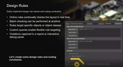
A constraint-based approach to PCB design is crucial in today's electronics industry. This article delves deeper into this complex and interesting topic, exploring various types of constraints, their advantages, and providing guidance on implementing them into your PCB design process.

Read More
Blog • Jan 23, 2024
Pi.MX8 Project – Introduction and Overview

Do you have extensive knowledge about the Pi.MX8 module? We're excited to introduce a new series of articles focusing on an innovative approach to utilizing this module. In this inaugural chapter, we provide insights into the preparation for this project and detail the elements that will be used.

Read More
Connect Procurement and Engineering Cover Photo
Blog • Jan 22, 2024
How to 'Shift Left' and Connect Procurement and Engineering? Altium 365 BOM Portal Step-by-Step

Learn why BOM management is critical for both procurement managers and electronic engineers. Altium 365 BOM Portal helps to bridge the gap between these worlds. Discover how!

Read More
Blog • Jan 10, 2024
Altium 365 Assembly Assistant: Available Now in the Altium Store

Happy New Year! 🎉 We are thrilled to announce that the Altium 365 Assembly Assistant is now officially released and available for direct purchase through the Altium Store.

Read More
Blog • Jan 9, 2024
Simple Documentation for Hand PCB Assembly

Creating documentation for hand PCB assembly does not prevent the same documentation from being utilized to assist in automated PCB assembly. Learn more about the optimal format for this data to enhance both your hand PCB assembly and overall assembly processes.

Read More
Blog • Jan 8, 2024
Constraint Manager: Precision in Every Detail

Explore the powerful features of Altium Designer 24! Experience Constraint Manager and revolutionize your PCB design with reusable constraint sets, schematic-to-board rule transition, easy class and differential pair grouping, and more.

Read More
Accelerate Last-Minute Design Changes Cover Photo
Blog • Dec 21, 2023
Accelerate Last-Minute Design Changes with Altium 365

Curious about how to solve production blockers before they derail your product launch? Explore how Altium 365® can help you swiftly manage last-minute design changes.

Read More
  • Show More
Tag (field_common_tag)
Embedded thumbnail for DFM and fab cost/time constraints: What is annular ring and how to configure it
How-To's • Jan 18, 2023
DFM and fab cost/time constraints: What is annular ring and how to configure it

The minimum dimension from the wall of the aperture to the edge of the pad is called an annular ring, and we can configure it with Altium Designer. We’ll show you how to get started and manage the annular ring in your design rules.

Start Watching
Embedded thumbnail for Altium 365 Getting Started: Gerber Compare
How-To's • Jan 16, 2023
Altium 365 Getting Started: Gerber Compare

The task of comparing different versions of manufacturing files usually arises when the electrical engineer needs to check and confirm the manufacturer's edits or clarify details of changes before starting production. In Altium 365 you can perform an automatic comparison of Gerber files.

Start Watching
Embedded thumbnail for Installing and Licensing Altium Designer
AD Get Started • Jan 9, 2023
Installing and Licensing Altium Designer
  • Altium Live Account
  • Downloading and Installing Altium Designer
  • Licensing Your Altium Designer
  • Activating Altium 365 Workspace
Start Watching
Embedded thumbnail for Video Series Introduction
AD Get Started • Jan 9, 2023
Video Series Introduction
  • Introduction of Altium Designer and Overview of the Next Modules
  • Presentation of Resources and Links to Help You Start with Altium Designer
Start Watching
Embedded thumbnail for New Project, Configuration, and Unified Environment
AD Get Started • Jan 9, 2023
New Project, Configuration, and Unified Environment
  • Unified Environment Platform
  • Configuration and Settings
  • Starting a New Project
Start Watching
Embedded thumbnail for Output Job File and Project Releaser
AD Get Started • Jan 9, 2023
Output Job File and Project Releaser
Output Job File
  • Output Job File Output Documents
  • Output Job File Environment, Outputs, and Output Containers
  • Generation of Output Job Files
Project Releaser
  • Initiating Project Release Environment
  • Preparation and Setup
  • Execution of the Releaser and Where Files Are Located for Manufacturer Use and Sending
Start Watching
Embedded thumbnail for PCB Editor, Transferring Schematic to PCB, Design Rules, Layer Stack Manager, and Routing
AD Get Started • Jan 9, 2023
PCB Editor, Transferring Schematic to PCB, Design Rules, Layer Stack Manager, and Routing
  • Transferring Schematic to PCB Editor
  • Editor Environment and Preparation
  • Board Shape and Size
  • Layer Stack Manager
  • Design Rules
  • Board Routing
Start Watching
Embedded thumbnail for Schematic Editor and Component Usage Management and Menus
AD Get Started • Jan 9, 2023
Schematic Editor and Component Usage Management and Menus
  • Altium Designer Schematic Editor
  • Schematic Types (Hierarchical and Flat) and Adding Schematics to Your Project
  • Proper Use of Net Labels and Ports
Start Watching
Embedded thumbnail for Polygon Pours
Working with Polygons • Jan 2, 2023
Polygon Pours

Polygon pours are used to create copper geometries on your board. You can prioritize polygon pour order, hide them to make it easier to work on your board, and repour them to resolve design rule conflicts.

Start Watching
Embedded thumbnail for How to Use the MCAD CoDesigner?
How-To's • Dec 30, 2022
How to Use the MCAD CoDesigner?

This video shows how the ECAD and MCAD engineers now can communicate directly while staying within their own design environment. The MCAD engineer is able to push design information directly from their design software straight into Altium Designer. Any changes can be reviewed, accepted, or denied by the receiving party. This process of pushing and reviewing design changes is bi-directional, meaning that both the MCAD or ECAD engineer can push and review changes to the other. 

Start Watching
Embedded thumbnail for Creating Additional Snap Points Using a 3D Model
How to use Snapping • Dec 28, 2022
Creating Additional Snap Points Using a 3D Model

Demonstration of using snap points with 3D models and how they can assist in the placement of said models.

Start Watching
Embedded thumbnail for Learn how Kärcher Developed Their First Autonomous Scrubber Drier with Altium 365
Success Stories • Dec 27, 2022
Learn how Kärcher Developed Their First Autonomous Scrubber Drier with Altium 365

Watch and see how Kärcher innovates faster and develops quality products by being able to work efficiently with interdisciplinary teams across the world to maintain its standards for the highest quality.

Start Watching
Embedded thumbnail for Polygon Connect Styles
Working with Polygons • Dec 26, 2022
Polygon Connect Styles

Define how vias and pads connect to polygons with a design rule. Customize the thermal relief width, number, and rotation as well as the air gap width.

Start Watching
Embedded thumbnail for How to work with Component Classes?
How to Work with Classes • Dec 23, 2022
How to work with Component Classes?

Modern printed circuit boards can contain a large number of components, which makes them difficult to work with. In this video we will show what component classes can be on a PCB, how to create custom component classes and how they can be useful for us. 

Start Watching
Embedded thumbnail for Create and Snap to a Circular Grid (Polar Grid)
How to use Snapping • Dec 19, 2022
Create and Snap to a Circular Grid (Polar Grid)

Instructional on how to create polar grids, how to snap to them, and why you might want to use them.

Start Watching
Embedded thumbnail for How to Connect Polygons to Nets
Working with Polygons • Dec 16, 2022
How to Connect Polygons to Nets

This video covers how to easily connect a polygon to a net using just two clicks. With the Properties panel open and a polygon selected, click the "Assign net" button in the Properties panel.

Start Watching
  • Show More
Tag (field_common_tag)
Altium Enterprise
On-Demand Webinar • May 10, 2025
Streamline your customer relation with Altium 365 Enterprise
Join our webinar designed for engineers and users in EMS companies
Watch Now
PCB
On-Demand Webinar • May 1, 2025
Altium Designer Overview
Altium Designer is the #1 PCB design tool for a reason. Join us for this live webinar and get an inside look at Altium’s world-class PCB design solution. See for yourself why design teams around the globe are making the switch to Altium Designer. Register now!
Watch Now
Enterprise
On-Demand Webinar • Apr 25, 2025
Altium Customization with Scripting or Low-Code
See how scripting, low-code, no-code, and API integrations can help you work more efficiently—without extra setup or complex systems.
Watch Now
A365 Webinar: Altium BOM Portal - From PCB Design to Parts Ordering in Minutes
On-Demand Webinar • Apr 21, 2025
Altium 365 BOM Portal - From PCB Design to Parts Ordering in Minutes
Join us to learn how to reduce sourcing time by up to 70% using Altium 365 BOM Portal.
Watch Now
April 2025 COM Webinar
On-Demand Webinar • Apr 17, 2025
Advanced xSignal and Impedance Control Techniques
We are hosting a free webinar on advanced xSignal configuration and impedance control techniques in Altium Designer to help you tackle signal integrity challenges. Register now to enhance your design skills.
Watch Now
Altium Enterprise
On-Demand Webinar • Mar 25, 2025
Unlocking the full potential of your design team with Altium's enterprise solution
See how Altium's enterprise solution can help you meet your electronic product design goals
Watch Now
Transmission line
On-Demand Webinar • Mar 4, 2025
Optimizing Layer Stackup and Impedance for High-Speed PCB Design
Learn how to master the layer stack manager to efficiently create stackups, manage materials, and ensure optimal design performance.
Watch Now
Harness design
On-Demand Webinar • Mar 2, 2025
Design Smarter - Harness, Multi-board, and MCAD CoDesign in Action
Discover how the latest Harness, Multi-board, and MCAD CoDesign tools can revolutionize your PCB design workflow.
Watch Now
ADv25
On-Demand Webinar • Jan 30, 2025
6 Reasons to Switch Design Tools
Come see how Altium Designer, the industry standard for PCB design, combined with Altium 365 delivers the world’s first connected PCB design experience.
Watch Now
PCB CoDesign
On-Demand Webinar • Jan 29, 2025
Level Up Your Team's Productivity with Altium
Discover how to create an efficient, collaborative, and transparent design process for your team!
Watch Now
Assembly variants
On-Demand Webinar • Jan 9, 2025
Designing with Assembly Variants
Join us to learn best practices and get into the details about setting up variants in your designs and speeding up your project development.
Watch Now
Single layer PCB
On-Demand Webinar • Jan 8, 2025
Optimized for Success - Advanced PCB Features in Altium Designer
This webinar will show you how to use the latest PCB Layout, signal integrity analysis, and component management design tools in Altium Designer.
Watch Now
Rigid flex
On-Demand Webinar • Dec 19, 2024
How To Use Modern Rigid-Flex Substrates
Join us in this webinar where we’ll go over how you can easily create your own flex design.
Watch Now
Power Analyzer
On-Demand Webinar • Oct 29, 2024
Power Integrity Made Simple
Power Analyzer by Keysight in Altium Designer makes it easy to resolve PDN issues that arise during the board design process within a unified design environment.
Watch Now
Electronic Component Traceability
On-Demand Webinar • Oct 25, 2024
Ensuring Electronic Component Traceability From Idea to Innovation
Watch the webinar to learn how to achieve full transparency, improve collaboration, and ensure compliance throughout your entire supply chain—whether you are sourcing domestically or abroad.
Watch Now
Why Altium Designer is Your Next Step for PCB Design
On-Demand Webinar • Oct 24, 2024
Why Altium Designer is Your Next Step for PCB Design
Join us to see how moving to Altium Designer can enable resilient and scalable designs while streamlining your entire workflow.
Watch Now
  • Show More
Tag (field_common_tag)
Loading
Loading...
Share link
Share with
Search by Update
Version
Update
25 26 24 23 22
25.0 25.1 25.2 25.3 25.4 25.5 25.6 25.7 25.8 25.9
26.1 26.2
24.10 24.9 24.8 24.7 24.6 24.5 24.4 24.3 24.2 24.1 24.0
23.11 23.10 23.9 23.8 23.7 23.6 23.5 23.4 23.3 23.2 23.1 23.0
22.11 22.10 22.9 22.8 22.7 22.6 22.5 22.4 22.3