
Main navigation

  • Home
  • Discover
  • Learning Center
  • What’s New

Second main navigation

  • Altium Community
  • Support
  • Documentation
×

Results

  • Updates
  • Blog 569
  • Video 539
  • Webinar 86
  • Playlist 53
Filters:
Tag (field_common_tag)
Blog • Oct 30, 2025
What Is BOM Management? A Practical Guide to Avoiding Costly Part Mismatches

From design to production, effective Bill of Materials (BOM) management is critical to ensuring smooth collaboration between engineering, procurement, and manufacturing teams. In this practical guide, we break down proven strategies for structuring, maintaining, and synchronizing your BOM to prevent costly mistakes and accelerate time-to-market.

Read More
Blog • Oct 29, 2025
Requirements Portal Introductory Tutorials

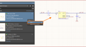
This series of guided demos shows how the Altium Requirements Portal transforms scattered requirement spreadsheets and emails into traceable, version-controlled data that stays aligned with your PCB design efforts.

Read More
Embedded thumbnail for PCB Design Tools for Every Team Size: Altium's New Approach
How-To's • Oct 28, 2025
PCB Design Tools for Every Team Size: Altium's New Approach

Explore how Altium is transforming PCB design with software solutions built for teams of every size. In this exclusive PCB West 2025 interview, Justin Sears highlights the key distinctions between Altium Develop and Altium Agile helping you identify the ideal platform for your design needs.

Start Watching
Blog • Oct 27, 2025
Bridging the Gap: When to Use Rigid-Flex Instead of Flex & Connector

Discover when a rigid-flex PCB is a better choice than a separate flex circuit and connector, especially for designs requiring compact packaging, repeated motion or high reliability. The article emphasizes that although rigid-flex needs more upfront planning and fabrication collaboration, it often pays off in simpler assemblies and improved performance.

Read More
Embedded thumbnail for PCB Design: Sequential Lamination vs Sub-Lamination
How-To's • Oct 23, 2025
PCB Design: Sequential Lamination vs Sub-Lamination

Explore the key distinctions between sequential lamination and sub-lamination techniques, and learn how each approach influences microvia placement, board complexity, and design flexibility in high-density interconnect (HDI) circuit board fabrication.


Start Watching
Blog • Oct 22, 2025
Bridging Mechanical and Electrical Teams for Smarter Automotive Design

As vehicles evolve into advanced electronic systems, the separation between electrical and mechanical design teams becomes a critical bottleneck. This article explores how synchronized ECAD–MCAD workflows help automotive projects move faster, reduce rework and maintain design integrity.

Read More
Embedded thumbnail for PCB Design Review: Power Meter Layout Deep Dive
How-To's • Oct 21, 2025
PCB Design Review: Power Meter Layout Deep Dive

Gain practical insights into PCB design with an in-depth power meter project review, covering parameter optimization, BOM control, and IPC-compliant high-voltage spacing.

Start Watching
Blog • Oct 20, 2025
Via Structures: Designing for Reliability, Not Just Density

We all want to pack more into our PCB designs, but the smallest via isn’t always the smartest one. Dive in to learn how picking the right structure can save you headaches down the line.

Read More
Embedded thumbnail for Drawing Tools for Pro Schematics in Altium
How-To's • Oct 16, 2025
Drawing Tools for Pro Schematics in Altium

In our brand-new tutorial, you’ll learn how to create professional-looking schematics in Altium using built-in drawing tools and features. We’ll show you how to add custom title blocks, revision histories, tables of contents, block diagrams, and color schemes to make your schematics stand out.

Start Watching
Blog • Oct 15, 2025
How Structural Electronics Enables 3D, Flexible, and Wearable Integration

Structural electronics integrates electronic functionality directly into the physical structure of a product, eliminating the need for traditional circuit boards. This article examines how advances in materials, additive manufacturing, and flexible substrates are enabling compact, 3D, and wearable systems with enhanced performance and design freedom.

Read More
Embedded thumbnail for 3 GHz RF Amplifier Deep Dive
How-To's • Oct 14, 2025
3 GHz RF Amplifier Deep Dive

Check out our design review of a 3.6 GHz RF amplifier! This in-depth analysis highlights schematic issues, PCB layout challenges, and key RF design principles to help you build better high-frequency circuits.

Start Watching
Blog • Oct 9, 2025
Beyond Traces: Why Soldermask May Be the Critical Factor in Ultra HDI

In ultra-HDI designs, soldermask is no longer a passive coating but a pivotal element that can determine manufacturability. This article explores why mask registration, resolution, and feature tolerances become critical as line spacings shrink below 50 µm.

Read More
Embedded thumbnail for The Right Way to Use SIG/GND/PWR/SIG Stackups
How-To's • Oct 8, 2025
The Right Way to Use SIG/GND/PWR/SIG Stackups

Find out how to properly implement signal-ground-power-signal stackups in 4-layer PCB designs. Check out our tutorial from Zach Peterson, where he explains when to use dedicated power layers, how to route signals correctly over split power planes, and common mistakes to avoid for optimal EMI performance and signal integrity.

Start Watching
Blog • Oct 7, 2025
How ECAD-MCAD Co-Design Supports Aerospace Reliability and Compliance

When the margin for error is nearly zero, aerospace engineering demands a design process that’s seamless across all domains. Here, we explore how ECAD-MCAD co-design delivers an integrated workflow that supports first-pass success and compliance with strict aerospace standards.

Read More
Embedded thumbnail for Altium Training - Design Environment: Documents and Panels
Altium Training • Oct 6, 2025
Altium Training - Design Environment: Documents and Panels

In our new tutorial, we explore different panel display modes, including docked, floating, and tabbed grouping arrangements. Effective panel management is essential for creating an efficient design environment tailored to your specific workflow requirements.

Start Watching
Blog • Oct 2, 2025
Most Common Causes of PCB Assembly Rework and Scrap

Many PCB assemblies fail not because of exotic faults, but due to basic issues like incorrect BOM entries or footprint mismatches that force rework or scrap. This article dives into the most common causes and how to prevent costly defects in your design-to-manufacturing process.

Read More
  • Show More
Tag (field_common_tag)
Cloud PLM Integration Altium 365 Blog Cover
Blog • May 27, 2024
6 Challenges of Managing Disconnected PLM Workflows

Discover six challenges of managing disconnected PLM workflows in electronics product development. Identify your main challenge and find the solution here.

Read More
Blog • May 21, 2024
DC-Aware Return Current in Mixed Signal PCBs

In this article, we will examine specific cases involving these types of components, where a very low-frequency signal or a DC signal needs to be measured, and the return path must be tracked to ensure the current loop is tight.

Read More
Blog • May 16, 2024
How to Create a PCB Panel Fabrication Drawing in Draftsman

PCB panels need a fabrication drawing, just like any other PCB that will go into production. Learn how to prepare panel drawings in our brand-new article about this part of the process.

Read More
Blog • May 13, 2024
PCB Layout Replication: The Perfect Tool for Test Jigs

Replicate your circuits across multiple blocks with just a few clicks using a flawless preview pane, ensuring consistent, perfect results without the need for trial and error. Check out our new article on the PCB Layout Replication feature.

Read More
Blog • May 8, 2024
Durability of Pin Plating Materials for PCB Connectors

Pin headers are common components in PCBs, yet one specification often overlooked is the plating material. Discover more about plating materials for electrical connectors in our latest article.

Read More
Altium 365 GovCloud Why We Chose AWS GovCloud (US) Cover
Blog • May 6, 2024
4 Reasons Why We Chose AWS GovCloud (US) for Altium 365 GovCloud

In this blog, we explain the reasons behind our decision to operate Altium 365 GovCloud within AWS GovCloud (US). This partnership is guided by a clear vision: to provide our users with a secure, compliant, and reliable platform for sensitive electronics design data.

Read More
Blog • Apr 30, 2024
How to Reduce Noise From Magnetostriction in Magnetic Components

Magnetic components driven by an AC signal can exhibit an irritating property due to magnetostriction - an effect causing vibrations in magnetic materials, resulting in audible sound. Explore this phenomenon further and discover methods to minimize its impact.

Read More
Blog • Apr 26, 2024
3D MID Design Whitepaper

Dive into a dynamic design experience where you can visualize and edit your circuits in true 3D, offering unparalleled precision. Altium Designer's 3D-MID (Mechatronic Integrated Device) Design tool revolutionizes the design process, providing a fresh perspective. Explore the capabilities and benefits of this feature in our comprehensive guide.

Read More
Blog • Apr 25, 2024
Types of Wiring Harnesses for Electronics

In today's world, many products utilize multiple PCBs interconnected with each other, often leading to a complex network of cables within an enclosure. The most effective way to manage these wires and cables is by constructing a wiring harness. This article explores the various types of harnesses used in electronics.

Read More
Advantages of Z2Data Integration You Can't Ignore Cover
Blog • Apr 23, 2024
5 Advantages of Z2Data Integration You Can't Ignore

Z2Data Integration in Altium 365 offers a practical way forward for engineering and procurement. Here are the top five advantages that can streamline your workflows.

Read More
Blog • Apr 22, 2024
Leveraging Altium Designer's Capabilities: Transforming PCB Design Data Management

Are you curious about how Altium Designer's PLM integration is revolutionizing electronics design? Bid farewell to inefficiencies and expensive revisions, and embark on discovering the cutting-edge approach to managing design data. Dive into our latest article to learn how to leverage this new standard in design data management.

Read More
Blog • Apr 19, 2024
Start Altium Designer 24 Training for Free

Level up your design skills with Altium Designer 24 training! Whether you're looking to brush up on the basics or delve into advanced techniques, our instructor-led or on-demand videos will help you master the latest features.

Read More
How Altium 365 Supports Agile Hardware Development
Blog • Apr 17, 2024
How Altium 365 Supports Agile Hardware Development

Discover how Altium 365 can be your ally in making agile hardware development a practical reality.

Read More
Blog • Apr 16, 2024
PCB Layout Replication Whitepaper

Experience seamless acceleration in your design workflow with Altium Designer® 24's PCB Layout Replication feature. Effortlessly duplicate layouts for recurring circuit blocks and component groups, amplifying efficiency and reducing expenses.

Read More
Altium 365 GovCloud 
How Is Your Design Data Protected
Blog • Apr 11, 2024
How Is Your Design Data Protected in Altium 365 GovCloud?

Here's how Altium 365 GovCloud protects your sensitive electronics design data. Learn more about our encryption technologies, access restrictions, and network security standards.

Read More
Budget and Data Security for IT Managers Cover
Blog • Apr 9, 2024
Balancing Budget and Data Security: Cost-Effective Strategies for IT Managers

Make decisions that balance cost-efficiency with uncompromised security. Find ways to ensure your data security measures are both strong and economically viable.

Read More
  • Show More
Tag (field_common_tag)
Embedded thumbnail for Drawing Tools for Pro Schematics in Altium
How-To's • Oct 16, 2025
Drawing Tools for Pro Schematics in Altium

In our brand-new tutorial, you’ll learn how to create professional-looking schematics in Altium using built-in drawing tools and features. We’ll show you how to add custom title blocks, revision histories, tables of contents, block diagrams, and color schemes to make your schematics stand out.

Start Watching
Embedded thumbnail for 3 GHz RF Amplifier Deep Dive
How-To's • Oct 14, 2025
3 GHz RF Amplifier Deep Dive

Check out our design review of a 3.6 GHz RF amplifier! This in-depth analysis highlights schematic issues, PCB layout challenges, and key RF design principles to help you build better high-frequency circuits.

Start Watching
Embedded thumbnail for The Right Way to Use SIG/GND/PWR/SIG Stackups
How-To's • Oct 8, 2025
The Right Way to Use SIG/GND/PWR/SIG Stackups

Find out how to properly implement signal-ground-power-signal stackups in 4-layer PCB designs. Check out our tutorial from Zach Peterson, where he explains when to use dedicated power layers, how to route signals correctly over split power planes, and common mistakes to avoid for optimal EMI performance and signal integrity.

Start Watching
Embedded thumbnail for Altium Training - Design Environment: Documents and Panels
Altium Training • Oct 6, 2025
Altium Training - Design Environment: Documents and Panels

In our new tutorial, we explore different panel display modes, including docked, floating, and tabbed grouping arrangements. Effective panel management is essential for creating an efficient design environment tailored to your specific workflow requirements.

Start Watching
Embedded thumbnail for Mechanically Drilled Blind & Buried Vias: PCB Design Rules Explained
How-To's • Oct 1, 2025
Mechanically Drilled Blind & Buried Vias: PCB Design Rules Explained

Discover the essential design rules and manufacturing processes for mechanically drilled blind and buried vias in PCB layouts in this comprehensive tutorial. We cover the stack drill-and-plate fabrication process, aspect ratio limitations, sub-lamination design, and copper weight considerations. You’ll also learn how these vias differ from HDI microvias and gain a clear understanding of the critical design constraints needed for successful PCB manufacturing.

Start Watching
Embedded thumbnail for Altium Training - Design Environment: Navigation with Schematic Workspace
Altium Training • Sep 29, 2025
Altium Training - Design Environment: Navigation with Schematic Workspace

Discover the most important navigation techniques for the schematic workspace using both mouse and keyboard controls. In this tutorial video, you’ll learn how to use the View menu commands for document fitting, area zooming, and object selection, along with advanced navigation shortcuts. Master mouse-based panning and zooming, explore Ctrl key combinations, and practice arrow key movements - all designed to simplify your workflow in the PCB design process.

Start Watching
Embedded thumbnail for Altium Training - Design Environment: The Altium Environment
How-To's • Sep 23, 2025
Altium Training - Design Environment: The Altium Environment

Get familiar with the core workspace layout and navigation methods. In this video, you’ll see how to open schematic and PCB documents, work within the unified design environment, and move between multiple open files using document tabs and keyboard shortcuts.

Start Watching
Embedded thumbnail for Altium Training - Design Environment: Opening a Project from a Local Drive
Altium Training • Sep 18, 2025
Altium Training - Design Environment: Opening a Project from a Local Drive

Get your PCB design workflow off to a smooth start. This Altium tutorial walks you through opening projects from your local directory - a core skill that keeps your process efficient and organized from day one.

Start Watching
Embedded thumbnail for Altium Essentials: Design Environment
Altium Training • Sep 16, 2025
Altium Essentials: Design Environment

Take control of your PCB design workflow with Altium Essentials: Design Environment. This tutorial module guides you through the fundamentals of workspace management, from handling panels and documents to mastering menus, context commands, and time-saving shortcuts.

Start Watching
Embedded thumbnail for What Makes a Great PCB Design Review Submission?
How-To's • Sep 11, 2025
What Makes a Great PCB Design Review Submission?

Turn your PCB designs into professional-grade submissions. At Altium, we reveal the key practices that transform schematics, layouts, and documentation into review-ready work that stands out. Watch our brand-new tutorial and take your PCB design process to the next level.

Start Watching
Embedded thumbnail for Altium Training - Workspace Folder Structure: Opening the Explorer Panel
Altium Training • Sep 9, 2025
Altium Training - Workspace Folder Structure: Opening the Explorer Panel

Discover the key ways to access the Explorer panel in Altium Designer with this step-by-step tutorial. The video walks you through four different methods, giving you the freedom to choose the approach that best fits your workflow.

Start Watching
Embedded thumbnail for Altium Essentials: Workspace Folder Structure Overview
Altium Training • Sep 3, 2025
Altium Essentials: Workspace Folder Structure Overview

Altium Essentials: Workspace Folder Structure is a tutorial series designed for PCB designers who are learning the fundamentals of navigating an Altium workspace. This playlist walks through key Explorer panel skills, including multiple ways to open it (via keyboard shortcuts, menus, panel buttons, and workspaces), navigating projects, and understanding the panel’s six core information areas.

Start Watching
Embedded thumbnail for NFC Reader Project Part One: Schematics to PCB in Altium
How-To's • Aug 28, 2025
NFC Reader Project Part One: Schematics to PCB in Altium

Check out our new, in-depth NFC Reader Project tutorial! In this two-part video series, we design an ESP32-based NFC transceiver board from schematics to PCB layout. In Part 1, we dive into the TRF7970A NFC chip from Texas Instruments and guide you step-by-step through the complete design process in Altium.

Start Watching
Embedded thumbnail for HDI PCB Design Review: nRF52840 Via Sizing & Stack-Up Best Practices
How-To's • Aug 25, 2025
HDI PCB Design Review: nRF52840 Via Sizing & Stack-Up Best Practices

Explore key HDI design strategies, from calculating aspect ratios and optimizing pad diameters to managing drill tolerances and refining stack-ups for improved signal integrity. This comprehensive review highlights practical solutions to common HDI challenges, including via-in-pad layouts, clearance violations, and layer thickness adjustments for both mechanical and laser drilling processes.

Start Watching
Embedded thumbnail for 13 Common PCB Problems & How to Fix Them in Altium
How-To's • Aug 20, 2025
13 Common PCB Problems & How to Fix Them in Altium

Stop wasting time on manufacturing rework. This guide shows you how to set up Altium’s design rules to prevent the 13 PCB issues that most often derail production ensuring your boards are built right the first time.

Start Watching
Embedded thumbnail for What's Inside Your MCU Module?
How-To's • Aug 18, 2025
What's Inside Your MCU Module?

Are you curious about what’s inside a microcontroller module? Join us as we take a closer look at the Texas Instruments CC3235 Wi-Fi module under the microscope. In this video, we’ll explore its key components, including the microcontroller, flash memory, and RF circuitry, and explain how they work together to power the module.

Start Watching
  • Show More
Tag (field_common_tag)
ADv25
On-Demand Webinar • Oct 24, 2024
Modernizing Engineering Workflows: Altium Designer 25 and the Future of Concurrent Design
Struggling with team misalignment and design errors? Join our exciting webinar to discover the groundbreaking advancements in Altium Designer 25!
Watch Now
KiCad Webinar
On-Demand Webinar • Oct 16, 2024
Taking the Next Step: Growing Beyond KiCad with Altium
Join our upcoming webinar to discover how Altium Designer can transition your KiCad projects without any data loss
Watch Now
Synchronize to Optimize Jira Integration
On-Demand Webinar • Oct 7, 2024
Synchronize to Optimize: Enhancing Efficiency with Jira Integration for Altium 365
Tired of juggling multiple tools for project management? Watch the webinar and see how Jira Integration for Altium 365 can optimize your workflows.
Watch Now
Wire bonding
On-Demand Webinar • Sep 29, 2024
Unlock New Design Possibilities with Wire Bonding
Explore how wire bonding can enhance your designs, provide size reduction, improve power management, and increase mechanical reliability.
Watch Now
routing
On-Demand Webinar • Sep 29, 2024
Advanced Routing Features & Techniques
To help you get the most out of your experience with Altium Designer, join our webinar this month and learn advanced routing techniques.
Watch Now
signal analyzer
On-Demand Webinar • Sep 25, 2024
Signal Integrity Made Simple
Discover how to easily detect and resolve high-speed signal integrity challenges without the need for extensive expertise.
Watch Now
competitive-displacement-webinar-3
On-Demand Webinar • Sep 20, 2024
Mastering Design Complexity: How Altium Designer Outperforms Cadence in Solving Workflow and Engineering Challenges - Part 2
Join our webinar to learn how to enhance efficiency, foster better collaboration, and accelerate your time-to-market with Altium unified solutions.
Watch Now
Breaking Down Silos Webinar
On-Demand Webinar • Sep 16, 2024
Breaking Down Data Silos: A Practical Comparison of Altium and Cadence in Cross-Functional PCB Design
Join us for a webinar that addresses the critical challenges of maintaining design data continuity across various design functions.
Watch Now
Draftsman
On-Demand Webinar • Sep 10, 2024
Mastering Design Complexity: How Altium Designer Outperforms Cadence in Solving Workflow and Engineering Challenges
Join our upcoming webinar to discover why engineers consistently choose Altium Designer as the standard in PCB design.
Watch Now
SPICE
On-Demand Webinar • Sep 3, 2024
Mastering SPICE Simulation in Altium Designer
Discover how the SPICE engine in Altium Designer can help you easily verify that your finished project functions as intended.
Watch Now
Output job
On-Demand Webinar • Aug 24, 2024
Beyond PCB Design with Altium Designer
In this webinar we'll dive into the essential aspects that go beyond the schematic and layout.
Watch Now
PCB
On-Demand Webinar • Aug 23, 2024
Elevate Your Design Skills: Tips & Tricks for Success
Discover practical insights and efficient methods that can enhance your PCB design capabilities.
Watch Now
Cyber Security Webinar Cover
On-Demand Webinar • Aug 6, 2024
The Anatomy of IT Compliance in Electronics Development: Altium 365 & AWS GovCloud
Are you an IT or security professional looking for a secure electronics design collaboration platform that could also support your ITAR and EAR compliance efforts? If so, watch this webinar to bring together the expertise of Altium 365 and AWS!
Watch Now
Design reuse
On-Demand Webinar • Aug 1, 2024
How to Speed-up Product Development with Reusable Circuitry
In this webinar you'll learn more about the benefits of the design reuse blocks approach as well as the Design Reuse panel.
Watch Now
Harness design
On-Demand Webinar • Jul 19, 2024
Stay Ahead of the Curve: A Half-Year Review of Altium Designer Improvements
Join our exciting webinar to discover the groundbreaking advancements in Altium Designer!
Watch Now
Lenght Tuning
On-Demand Webinar • Jun 26, 2024
Achieve Precision and Speed with Altium Designer 24's Innovative Routing Features
Speed up your routing process and achieve better results for even your most demanding designs.
Watch Now
  • Show More
Tag (field_common_tag)
Loading
Loading...
Share link
Share with
Search by Update
Version
Update
25 26 24 23 22
25.0 25.1 25.2 25.3 25.4 25.5 25.6 25.7 25.8 25.9
26.1 26.2
24.10 24.9 24.8 24.7 24.6 24.5 24.4 24.3 24.2 24.1 24.0
23.11 23.10 23.9 23.8 23.7 23.6 23.5 23.4 23.3 23.2 23.1 23.0
22.11 22.10 22.9 22.8 22.7 22.6 22.5 22.4 22.3