
Main navigation

  • Home
  • Discover
  • Learning Center
  • What’s New

Second main navigation

  • Altium Community
  • Support
  • Documentation
×

Results

  • Updates
  • Blog 569
  • Video 538
  • Webinar 86
  • Playlist 53
Filters:
Tag (field_common_tag)
Blog • Oct 29, 2025
Requirements Portal Introductory Tutorials

This series of guided demos shows how the Altium Requirements Portal transforms scattered requirement spreadsheets and emails into traceable, version-controlled data that stays aligned with your PCB design efforts.

Read More
Embedded thumbnail for PCB Design Tools for Every Team Size: Altium's New Approach
How-To's • Oct 28, 2025
PCB Design Tools for Every Team Size: Altium's New Approach

Explore how Altium is transforming PCB design with software solutions built for teams of every size. In this exclusive PCB West 2025 interview, Justin Sears highlights the key distinctions between Altium Develop and Altium Agile helping you identify the ideal platform for your design needs.

Start Watching
Blog • Oct 27, 2025
Bridging the Gap: When to Use Rigid-Flex Instead of Flex & Connector

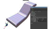
Discover when a rigid-flex PCB is a better choice than a separate flex circuit and connector, especially for designs requiring compact packaging, repeated motion or high reliability. The article emphasizes that although rigid-flex needs more upfront planning and fabrication collaboration, it often pays off in simpler assemblies and improved performance.

Read More
Embedded thumbnail for PCB Design: Sequential Lamination vs Sub-Lamination
How-To's • Oct 23, 2025
PCB Design: Sequential Lamination vs Sub-Lamination

Explore the key distinctions between sequential lamination and sub-lamination techniques, and learn how each approach influences microvia placement, board complexity, and design flexibility in high-density interconnect (HDI) circuit board fabrication.


Start Watching
Blog • Oct 22, 2025
Bridging Mechanical and Electrical Teams for Smarter Automotive Design

As vehicles evolve into advanced electronic systems, the separation between electrical and mechanical design teams becomes a critical bottleneck. This article explores how synchronized ECAD–MCAD workflows help automotive projects move faster, reduce rework and maintain design integrity.

Read More
Embedded thumbnail for PCB Design Review: Power Meter Layout Deep Dive
How-To's • Oct 21, 2025
PCB Design Review: Power Meter Layout Deep Dive

Gain practical insights into PCB design with an in-depth power meter project review, covering parameter optimization, BOM control, and IPC-compliant high-voltage spacing.

Start Watching
Blog • Oct 20, 2025
Via Structures: Designing for Reliability, Not Just Density

We all want to pack more into our PCB designs, but the smallest via isn’t always the smartest one. Dive in to learn how picking the right structure can save you headaches down the line.

Read More
Embedded thumbnail for Drawing Tools for Pro Schematics in Altium
How-To's • Oct 16, 2025
Drawing Tools for Pro Schematics in Altium

In our brand-new tutorial, you’ll learn how to create professional-looking schematics in Altium using built-in drawing tools and features. We’ll show you how to add custom title blocks, revision histories, tables of contents, block diagrams, and color schemes to make your schematics stand out.

Start Watching
Blog • Oct 15, 2025
How Structural Electronics Enables 3D, Flexible, and Wearable Integration

Structural electronics integrates electronic functionality directly into the physical structure of a product, eliminating the need for traditional circuit boards. This article examines how advances in materials, additive manufacturing, and flexible substrates are enabling compact, 3D, and wearable systems with enhanced performance and design freedom.

Read More
Embedded thumbnail for 3 GHz RF Amplifier Deep Dive
How-To's • Oct 14, 2025
3 GHz RF Amplifier Deep Dive

Check out our design review of a 3.6 GHz RF amplifier! This in-depth analysis highlights schematic issues, PCB layout challenges, and key RF design principles to help you build better high-frequency circuits.

Start Watching
Blog • Oct 9, 2025
Beyond Traces: Why Soldermask May Be the Critical Factor in Ultra HDI

In ultra-HDI designs, soldermask is no longer a passive coating but a pivotal element that can determine manufacturability. This article explores why mask registration, resolution, and feature tolerances become critical as line spacings shrink below 50 µm.

Read More
Embedded thumbnail for The Right Way to Use SIG/GND/PWR/SIG Stackups
How-To's • Oct 8, 2025
The Right Way to Use SIG/GND/PWR/SIG Stackups

Find out how to properly implement signal-ground-power-signal stackups in 4-layer PCB designs. Check out our tutorial from Zach Peterson, where he explains when to use dedicated power layers, how to route signals correctly over split power planes, and common mistakes to avoid for optimal EMI performance and signal integrity.

Start Watching
Blog • Oct 7, 2025
How ECAD-MCAD Co-Design Supports Aerospace Reliability and Compliance

When the margin for error is nearly zero, aerospace engineering demands a design process that’s seamless across all domains. Here, we explore how ECAD-MCAD co-design delivers an integrated workflow that supports first-pass success and compliance with strict aerospace standards.

Read More
Embedded thumbnail for Altium Training - Design Environment: Documents and Panels
Altium Training • Oct 6, 2025
Altium Training - Design Environment: Documents and Panels

In our new tutorial, we explore different panel display modes, including docked, floating, and tabbed grouping arrangements. Effective panel management is essential for creating an efficient design environment tailored to your specific workflow requirements.

Start Watching
Blog • Oct 2, 2025
Most Common Causes of PCB Assembly Rework and Scrap

Many PCB assemblies fail not because of exotic faults, but due to basic issues like incorrect BOM entries or footprint mismatches that force rework or scrap. This article dives into the most common causes and how to prevent costly defects in your design-to-manufacturing process.

Read More
Embedded thumbnail for Mechanically Drilled Blind & Buried Vias: PCB Design Rules Explained
How-To's • Oct 1, 2025
Mechanically Drilled Blind & Buried Vias: PCB Design Rules Explained

Discover the essential design rules and manufacturing processes for mechanically drilled blind and buried vias in PCB layouts in this comprehensive tutorial. We cover the stack drill-and-plate fabrication process, aspect ratio limitations, sub-lamination design, and copper weight considerations. You’ll also learn how these vias differ from HDI microvias and gain a clear understanding of the critical design constraints needed for successful PCB manufacturing.

Start Watching
  • Show More
Tag (field_common_tag)
Blog • May 6, 2025
New Routing Possibilities with Ultra HDI

Explore how Ultra HDI technology is redefining PCB design. This article breaks down the benefits and manufacturing considerations of Ultra HDI, and how it enables next-level routing density and miniaturization in advanced electronics.

Read More
Blog • May 5, 2025
3D-MID in Focus: Principles, Processes, and Practical Use

This article introduces 3D-MID (Mechatronic Integrated Devices), a technology that integrates circuitry into 3D plastic structures to reduce size, weight, and complexity. It explains the production process, use cases, and benefits of 3D-MID in sectors like automotive, medical, and consumer electronics.

Read More
Blog • Apr 30, 2025
Eliminate EMI and Signal Integrity Issues in Multi-Board PCB Designs

Ensure signal integrity and minimize EMI in complex electronics. Our new article explains how to address electromagnetic interference and signal integrity challenges in multi-board PCB designs, offering practical strategies and layout considerations for reliable system performance.

Read More
Blog • Apr 25, 2025
How to Overcome Power Distribution and Connector Misalignment Challenges in Multi-Board PCB Systems

Connector misalignment can compromise the reliability of power delivery in multi-board systems. This article explores the causes, effects, and prevention strategies for connector misalignment in power distribution, helping you design more robust multi-board PCB systems.

Read More
Blog • Apr 22, 2025
Mastering Component Templates in Altium Designer 25

Our new article by Dario Fresu explains how Component Templates in Altium Designer 25 Pro improve design consistency, reduce errors, and streamline collaboration. It highlights practical benefits like standardized naming, faster component creation, and scalability across projects. Includes examples of using templates with Altium 365™ to simplify complex component setup.

Read More
Blog • Apr 18, 2025
Wire Harness Design Guide for Development and Manufacturing

Designing a wire harness goes far beyond just connecting components—it’s about ensuring manufacturability, reliability, and compliance. This article walks you through the entire process, from initial design to production, helping you streamline development and avoid common pitfalls.

Read More
Blog • Apr 15, 2025
Preparing for Medical Device Cybersecurity Assessments

Explore the key considerations and best practices for conducting cybersecurity assessments in medical device development. This article outlines how to identify potential threats, evaluate risks, and ensure compliance with evolving industry standards.

Read More
Blog • Apr 8, 2025
Harness Complexity, Design with Simplicity

Harness Design in Altium Designer simplifies managing PCB interconnections, ensuring reliable performance and streamlined manufacturing. With logical connectivity tools, harness layout drawing, and manufacturing-ready documentation, it keeps your designs efficient and organized—all within a unified design environment. Perfect for automotive, aerospace, and industrial applications.

Read More
Blog • Apr 7, 2025
Getting Started with NVMe and the Raspberry Pi 5

Our new article guides you through enhancing your Raspberry Pi 5's performance by setting up NVMe SSD storage using an expansion HAT. It covers the benefits over traditional MicroSD cards, including improved speed and reliability, and provides step-by-step instructions for installation and configuration.

Read More
Blog • Apr 4, 2025
Why Human Error Is Electronics Design Cybersecurity's Biggest Weakness

Human error is a leading cause of cybersecurity breaches—even in electrical engineering. Our article explores how everyday design and collaboration habits can create vulnerabilities, and what engineers can do to build safer, more secure workflows.

Read More
Blog • Apr 2, 2025
From Concept to Production: A Modern Approach to Wire Harness Engineering

Discover how modern wire harness engineering is evolving to meet the growing complexity of electrified systems. This whitepaper explores best practices, intelligent automation, and ECAD-MCAD collaboration to improve efficiency and reduce errors. Download now to stay ahead in an increasingly connected world.

Read More
Blog • Mar 31, 2025
Transforming RF Design with Ultra HDI

Ultra-HDI technology is transforming RF design by enabling finer line widths, improved signal integrity, and more compact, high-performance boards. Our brand-new article explores its advantages over traditional methods and the benefits of integrating flexible circuits.

Read More
Blog • Mar 26, 2025
Boost Your PCB Testing Efficiency with Testpoint Manager

Testpoints are essential for efficient PCBA testing and debugging. Our latest whitepaper dives into testpoint optimization, fault detection, and automated testing strategies, along with a full tutorial on using Testpoint Manager in Altium Designer. Discover how to streamline your testpoint assignments and improve measurement accuracy!

Read More
Blog • Mar 24, 2025
Top 5 Hidden Challenges of Cable Harness Design in Electronic Products

Krishna Sundaram explores the hidden challenges of cable harness design, from routing complexity to mechanical constraints and manufacturability. Learn how to design a robust and efficient harness.

Read More
Blog • Mar 19, 2025
Ultra HDI: It’s Not Just Buzzword

Ultra-HDI technology is transforming PCB design, enabling unprecedented miniaturization and performance. In this article, explore what sets Ultra-HDI apart from traditional HDI and how it’s shaping the future of electronics.

Read More
Blog • Mar 17, 2025
Cloud PCB Design: 5 Cloud Security Myths Debunked

This article addresses common misconceptions about cloud security in PCB design. It explains how modern cloud platforms, such as Altium 365, often provide superior security compared to traditional on-premises solutions. Key features like advanced infrastructure, granular access controls, and compliance with stringent regulations ensure the protection of valuable design data.

Read More
  • Show More
Tag (field_common_tag)
Embedded thumbnail for 3 GHz RF Amplifier Deep Dive
How-To's • Oct 14, 2025
3 GHz RF Amplifier Deep Dive

Check out our design review of a 3.6 GHz RF amplifier! This in-depth analysis highlights schematic issues, PCB layout challenges, and key RF design principles to help you build better high-frequency circuits.

Start Watching
Embedded thumbnail for The Right Way to Use SIG/GND/PWR/SIG Stackups
How-To's • Oct 8, 2025
The Right Way to Use SIG/GND/PWR/SIG Stackups

Find out how to properly implement signal-ground-power-signal stackups in 4-layer PCB designs. Check out our tutorial from Zach Peterson, where he explains when to use dedicated power layers, how to route signals correctly over split power planes, and common mistakes to avoid for optimal EMI performance and signal integrity.

Start Watching
Embedded thumbnail for Altium Training - Design Environment: Documents and Panels
Altium Training • Oct 6, 2025
Altium Training - Design Environment: Documents and Panels

In our new tutorial, we explore different panel display modes, including docked, floating, and tabbed grouping arrangements. Effective panel management is essential for creating an efficient design environment tailored to your specific workflow requirements.

Start Watching
Embedded thumbnail for Mechanically Drilled Blind & Buried Vias: PCB Design Rules Explained
How-To's • Oct 1, 2025
Mechanically Drilled Blind & Buried Vias: PCB Design Rules Explained

Discover the essential design rules and manufacturing processes for mechanically drilled blind and buried vias in PCB layouts in this comprehensive tutorial. We cover the stack drill-and-plate fabrication process, aspect ratio limitations, sub-lamination design, and copper weight considerations. You’ll also learn how these vias differ from HDI microvias and gain a clear understanding of the critical design constraints needed for successful PCB manufacturing.

Start Watching
Embedded thumbnail for Altium Training - Design Environment: Navigation with Schematic Workspace
Altium Training • Sep 29, 2025
Altium Training - Design Environment: Navigation with Schematic Workspace

Discover the most important navigation techniques for the schematic workspace using both mouse and keyboard controls. In this tutorial video, you’ll learn how to use the View menu commands for document fitting, area zooming, and object selection, along with advanced navigation shortcuts. Master mouse-based panning and zooming, explore Ctrl key combinations, and practice arrow key movements - all designed to simplify your workflow in the PCB design process.

Start Watching
Embedded thumbnail for Altium Training - Design Environment: The Altium Environment
How-To's • Sep 23, 2025
Altium Training - Design Environment: The Altium Environment

Get familiar with the core workspace layout and navigation methods. In this video, you’ll see how to open schematic and PCB documents, work within the unified design environment, and move between multiple open files using document tabs and keyboard shortcuts.

Start Watching
Embedded thumbnail for Altium Training - Design Environment: Opening a Project from a Local Drive
Altium Training • Sep 18, 2025
Altium Training - Design Environment: Opening a Project from a Local Drive

Get your PCB design workflow off to a smooth start. This Altium tutorial walks you through opening projects from your local directory - a core skill that keeps your process efficient and organized from day one.

Start Watching
Embedded thumbnail for Altium Essentials: Design Environment
Altium Training • Sep 16, 2025
Altium Essentials: Design Environment

Take control of your PCB design workflow with Altium Essentials: Design Environment. This tutorial module guides you through the fundamentals of workspace management, from handling panels and documents to mastering menus, context commands, and time-saving shortcuts.

Start Watching
Embedded thumbnail for What Makes a Great PCB Design Review Submission?
How-To's • Sep 11, 2025
What Makes a Great PCB Design Review Submission?

Turn your PCB designs into professional-grade submissions. At Altium, we reveal the key practices that transform schematics, layouts, and documentation into review-ready work that stands out. Watch our brand-new tutorial and take your PCB design process to the next level.

Start Watching
Embedded thumbnail for Altium Training - Workspace Folder Structure: Opening the Explorer Panel
Altium Training • Sep 9, 2025
Altium Training - Workspace Folder Structure: Opening the Explorer Panel

Discover the key ways to access the Explorer panel in Altium Designer with this step-by-step tutorial. The video walks you through four different methods, giving you the freedom to choose the approach that best fits your workflow.

Start Watching
Embedded thumbnail for Altium Essentials: Workspace Folder Structure Overview
Altium Training • Sep 3, 2025
Altium Essentials: Workspace Folder Structure Overview

Altium Essentials: Workspace Folder Structure is a tutorial series designed for PCB designers who are learning the fundamentals of navigating an Altium workspace. This playlist walks through key Explorer panel skills, including multiple ways to open it (via keyboard shortcuts, menus, panel buttons, and workspaces), navigating projects, and understanding the panel’s six core information areas.

Start Watching
Embedded thumbnail for NFC Reader Project Part One: Schematics to PCB in Altium
How-To's • Aug 28, 2025
NFC Reader Project Part One: Schematics to PCB in Altium

Check out our new, in-depth NFC Reader Project tutorial! In this two-part video series, we design an ESP32-based NFC transceiver board from schematics to PCB layout. In Part 1, we dive into the TRF7970A NFC chip from Texas Instruments and guide you step-by-step through the complete design process in Altium.

Start Watching
Embedded thumbnail for HDI PCB Design Review: nRF52840 Via Sizing & Stack-Up Best Practices
How-To's • Aug 25, 2025
HDI PCB Design Review: nRF52840 Via Sizing & Stack-Up Best Practices

Explore key HDI design strategies, from calculating aspect ratios and optimizing pad diameters to managing drill tolerances and refining stack-ups for improved signal integrity. This comprehensive review highlights practical solutions to common HDI challenges, including via-in-pad layouts, clearance violations, and layer thickness adjustments for both mechanical and laser drilling processes.

Start Watching
Embedded thumbnail for 13 Common PCB Problems & How to Fix Them in Altium
How-To's • Aug 20, 2025
13 Common PCB Problems & How to Fix Them in Altium

Stop wasting time on manufacturing rework. This guide shows you how to set up Altium’s design rules to prevent the 13 PCB issues that most often derail production ensuring your boards are built right the first time.

Start Watching
Embedded thumbnail for What's Inside Your MCU Module?
How-To's • Aug 18, 2025
What's Inside Your MCU Module?

Are you curious about what’s inside a microcontroller module? Join us as we take a closer look at the Texas Instruments CC3235 Wi-Fi module under the microscope. In this video, we’ll explore its key components, including the microcontroller, flash memory, and RF circuitry, and explain how they work together to power the module.

Start Watching
Embedded thumbnail for Altium Harness Design Tutorial - From Schematic to 3D Layout
How-To's • Aug 12, 2025
Altium Harness Design Tutorial - From Schematic to 3D Layout

Design professional harness systems in Altium with confidence. Follow this comprehensive tutorial to learn multiboard project setup, create wiring diagrams, visualize in 3D, and produce manufacturing-ready documentation complete with ECAD-MCAD integration for precise wire length measurement.

Start Watching
  • Show More
Tag (field_common_tag)
 Preventing Obsolescence Before It Hits
On-Demand Webinar • Jun 12, 2025
Proactive Lifecycle Management: Preventing Obsolescence Before It Hits
Take the first step toward eliminating avoidable delays and costly redesigns. Don't miss it and register now!
Watch Now
Integrating Requirements June 2025 Webinar
On-Demand Webinar • May 28, 2025
Integrating Requirements into Your PCB Design Workflow
Join our webinar where you will learn about integrated requirements tools who can help you eliminate late-stage design changes, AI support through system requirements and integration of design requirements directly in PCB Design. Don't miss it, register now!
Watch Now
A365 Webinar
On-Demand Webinar • Apr 23, 2025
Collaborative Design Review: Ensuring Quality from Schematics to Supply Chain
Join our live webinar to learn how Altium 365 accelerates collaboration, standardizes workflows, and ensures design integrity to mitigate risks and accelerate time to market.
Watch Now
Webinar: From Prototype to Production: Optimizing BOM Costs Without Compromising Quality with Part Analytics
On-Demand Webinar • Apr 22, 2025
From Prototype to Production: Optimizing BOM Costs Without Compromising Quality with Part Analytics
Learn how to reduce production BOM costs without redesign, explore techniques to consolidate part demand for volume savings, and discover case examples from supply chain teams that increased sourcing process efficiency by up to 97%.
Watch Now
Streamlining Team Collaboration
On-Demand Webinar • Apr 17, 2025
Streamlining Team Collaboration in Industrial PCB Projects
Join us for our upcoming webinar to discover how Altium Designer and Altium 365 can transform your team’s collaboration and take your PCB design projects to the next level. Attend for a chance to win free access to the Altium 365 Training Bundle.
Watch Now
Component management
On-Demand Webinar • Apr 10, 2025
Ensure Best Designs with Professional Library Management
In this webinar, you'll discover how Altium Designer facilitates robust component management, including adding part choices to mitigate supply chain risks and leveraging Altium 365 managed components.
Watch Now
April 2025 Webinar Cover
On-Demand Webinar • Apr 9, 2025
Component Selection in Altium Designer: Making Data-Driven Decisions with Data Integrations
Improve component selection with real-time data insights in Altium 365! Join our live webinar to optimize your PCB development. Sign up now!
Watch Now
Altium Agile
Live Webinar
Altium Agile Teams - Sneak Peek
Get a first glimpse into this new Electronic Product Development Platform.
Jan
21
English
3:00 PM, CET
Jan
21
German
10:00 AM, CET
Jan
22
Italian
10:00 AM, CET
Jan
22
French
3:00 PM, CET
Jan
22
Spanish
3:00 PM, CET
Register Now
Altium Designer Overview
Live Webinar
Altium Designer Onboarding Workshop
Join our live training workshop and see Altium Designer in action—from creating your first schematic to delivering ready-to-manufacture PCB files.
Jan
15
English
2:00 PM, CET
Register Now
Altium Platform
On-Demand Webinar • Nov 21, 2025
Altium Platform - A foundation to meet your & your company’s targets
Discover how the Altium platform makes multidisciplinary cooperation easy and efficient.
Watch Now
Harness design
On-Demand Webinar • Nov 17, 2025
From single PCB to Harnessed Product
Discover how to streamline PCB-to-harness design with Altium’s powerful tools and boost collaboration across disciplines.
Watch Now
3D-MID Design
On-Demand Webinar • Oct 20, 2025
3D-MID Design in Altium
Discover how even complex products for 3D circuit designs are implemented easily in Altium.
Watch Now
Altium Designer Overview
On-Demand Webinar • Aug 20, 2025
Altium Designer and Altium 365 Overview
In this webinar we will show you how easy it is to create a prototype from scratch using Altium Designer in combination with Altium 365.
Watch Now
Altium Enterprise
On-Demand Webinar • Aug 3, 2025
Safety & Reliability in Electronics Design – Strategies, Standards & Tools
How can development teams and decision-makers effectively implement safety, security, and compliance without delaying innovation?
Watch Now
Altium Enterprise
On-Demand Webinar • Aug 2, 2025
Sustainability & Energy Efficiency in Electronic Product Development
Watch Now
Proactive Component Selection
On-Demand Webinar • May 22, 2025
Proactive Component Selection: Mitigating Manufacturing Delays Before They Happen
Most teams spend hours on component research yet still face redesigns. Learn how Altium 365 helps you make proactive, data-driven part decisions. Join SiliconExpert’s Jackie Sartin to discover smarter sourcing with real-time insights and validated alternatives.
Watch Now
  • Show More
Tag (field_common_tag)
Loading
Loading...
Share link
Share with
Search by Update
Version
Update
25 26 24 23 22
25.0 25.1 25.2 25.3 25.4 25.5 25.6 25.7 25.8 25.9
26.1 26.2
24.10 24.9 24.8 24.7 24.6 24.5 24.4 24.3 24.2 24.1 24.0
23.11 23.10 23.9 23.8 23.7 23.6 23.5 23.4 23.3 23.2 23.1 23.0
22.11 22.10 22.9 22.8 22.7 22.6 22.5 22.4 22.3