
Main navigation

  • Home
  • Discover
  • Learning Center
  • What’s New

Second main navigation

  • Altium Community
  • Support
  • Documentation
×

Results

  • Updates
  • Blog 571
  • Video 540
  • Webinar 86
  • Playlist 53
Filters:
Tag (field_common_tag)
Embedded thumbnail for Altium Develop: Returning to Our Roots
How-To's • Nov 5, 2025
Altium Develop: Returning to Our Roots

Lawrence Romine unveils Altium’s groundbreaking approach to product development with Altium Develop. This innovative solution realigns the company with its core mission - empowering individual engineers and small teams. Explore the strategic vision behind creating a product that seamlessly balances accessibility, robust functionality, and intuitive design.

Start Watching
Blog • Nov 4, 2025
6 Areas Your PCB Design Reviews Should Focus On

Learn the six essential topics every electronics team should address in design reviews to improve quality, avoid surprises and bring products to market faster.

Read More
Embedded thumbnail for Altium Training - Navigating Schematics: Schematic Preference Settings for Navigation
Altium Training • Nov 3, 2025
Altium Training - Navigating Schematics: Schematic Preference Settings for Navigation

Unlock smarter design navigation in Altium! Learn how to customize navigation preferences to boost your design insight and visualize connectivity like never before. In this video, we’ll explore Design Insight settings, interactive connectivity hover features, and quick thumbnail navigation between schematic sheets. All designed to make your workflow faster, clearer, and more intuitive.

Start Watching
Blog • Oct 30, 2025
What Is BOM Management? A Practical Guide to Avoiding Costly Part Mismatches

From design to production, effective Bill of Materials (BOM) management is critical to ensuring smooth collaboration between engineering, procurement, and manufacturing teams. In this practical guide, we break down proven strategies for structuring, maintaining, and synchronizing your BOM to prevent costly mistakes and accelerate time-to-market.

Read More
Blog • Oct 29, 2025
Requirements Portal Introductory Tutorials

This series of guided demos shows how the Altium Requirements Portal transforms scattered requirement spreadsheets and emails into traceable, version-controlled data that stays aligned with your PCB design efforts.

Read More
Embedded thumbnail for PCB Design Tools for Every Team Size: Altium's New Approach
How-To's • Oct 28, 2025
PCB Design Tools for Every Team Size: Altium's New Approach

Explore how Altium is transforming PCB design with software solutions built for teams of every size. In this exclusive PCB West 2025 interview, Justin Sears highlights the key distinctions between Altium Develop and Altium Agile helping you identify the ideal platform for your design needs.

Start Watching
Blog • Oct 27, 2025
Bridging the Gap: When to Use Rigid-Flex Instead of Flex & Connector

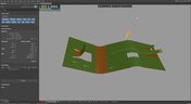
Discover when a rigid-flex PCB is a better choice than a separate flex circuit and connector, especially for designs requiring compact packaging, repeated motion or high reliability. The article emphasizes that although rigid-flex needs more upfront planning and fabrication collaboration, it often pays off in simpler assemblies and improved performance.

Read More
Embedded thumbnail for PCB Design: Sequential Lamination vs Sub-Lamination
How-To's • Oct 23, 2025
PCB Design: Sequential Lamination vs Sub-Lamination

Explore the key distinctions between sequential lamination and sub-lamination techniques, and learn how each approach influences microvia placement, board complexity, and design flexibility in high-density interconnect (HDI) circuit board fabrication.


Start Watching
Blog • Oct 22, 2025
Bridging Mechanical and Electrical Teams for Smarter Automotive Design

As vehicles evolve into advanced electronic systems, the separation between electrical and mechanical design teams becomes a critical bottleneck. This article explores how synchronized ECAD–MCAD workflows help automotive projects move faster, reduce rework and maintain design integrity.

Read More
Embedded thumbnail for PCB Design Review: Power Meter Layout Deep Dive
How-To's • Oct 21, 2025
PCB Design Review: Power Meter Layout Deep Dive

Gain practical insights into PCB design with an in-depth power meter project review, covering parameter optimization, BOM control, and IPC-compliant high-voltage spacing.

Start Watching
Blog • Oct 20, 2025
Via Structures: Designing for Reliability, Not Just Density

We all want to pack more into our PCB designs, but the smallest via isn’t always the smartest one. Dive in to learn how picking the right structure can save you headaches down the line.

Read More
Embedded thumbnail for Drawing Tools for Pro Schematics in Altium
How-To's • Oct 16, 2025
Drawing Tools for Pro Schematics in Altium

In our brand-new tutorial, you’ll learn how to create professional-looking schematics in Altium using built-in drawing tools and features. We’ll show you how to add custom title blocks, revision histories, tables of contents, block diagrams, and color schemes to make your schematics stand out.

Start Watching
Blog • Oct 15, 2025
How Structural Electronics Enables 3D, Flexible, and Wearable Integration

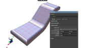
Structural electronics integrates electronic functionality directly into the physical structure of a product, eliminating the need for traditional circuit boards. This article examines how advances in materials, additive manufacturing, and flexible substrates are enabling compact, 3D, and wearable systems with enhanced performance and design freedom.

Read More
Embedded thumbnail for 3 GHz RF Amplifier Deep Dive
How-To's • Oct 14, 2025
3 GHz RF Amplifier Deep Dive

Check out our design review of a 3.6 GHz RF amplifier! This in-depth analysis highlights schematic issues, PCB layout challenges, and key RF design principles to help you build better high-frequency circuits.

Start Watching
Blog • Oct 9, 2025
Beyond Traces: Why Soldermask May Be the Critical Factor in Ultra HDI

In ultra-HDI designs, soldermask is no longer a passive coating but a pivotal element that can determine manufacturability. This article explores why mask registration, resolution, and feature tolerances become critical as line spacings shrink below 50 µm.

Read More
Embedded thumbnail for The Right Way to Use SIG/GND/PWR/SIG Stackups
How-To's • Oct 8, 2025
The Right Way to Use SIG/GND/PWR/SIG Stackups

Find out how to properly implement signal-ground-power-signal stackups in 4-layer PCB designs. Check out our tutorial from Zach Peterson, where he explains when to use dedicated power layers, how to route signals correctly over split power planes, and common mistakes to avoid for optimal EMI performance and signal integrity.

Start Watching
  • Show More
Tag (field_common_tag)
Using Altium 365 Over Your Vanilla Version Control System
Blog • Dec 20, 2021
Using Altium 365 Over Your Vanilla Version Control System

There are all sorts of version control systems out there that people have been using with their PCB design software. As discussed in Why Use a Version Control System, we looked at different options ranging for local hard drive storage to sophisticated online revisioning systems. In this article we will be reviewing the differences between a standard VCS and Altium 365.

Read More
Why Use a Version Control System in PCB Design
Blog • Dec 17, 2021
Why Use a Version Control System in PCB Design

Version Control Systems (VCS) have been around for many decades within the software world but can be surprisingly new to some folks in the electronics design industry. This article will cover what a VCS is, what it does, and why you should be using one for your PCB design projects.

Read More
IPC 6012 Class 3 Annular Ring
Blog • Dec 16, 2021
Meeting Standards: IPC 6012 Class 3 Annular Ring

Designers often conflate leftover annular ring and pad sizes - they need to place a sufficiently large pad size on the surface layer to ensure that the annular ring that is leftover during fabrication will be large enough. As long as the annular ring is sufficiently large, the drill hit will not be considered defective and the board will have passed inspection. In this article, I'll discuss the limits on IPC-6012 Class 3 annular rings as these are a standard fabrication requirement for high-reliability rigid PCBs.

Read More
PCB fabrication notes
Blog • Dec 14, 2021
Decoding PCB Fabrication Notes

Sending a board out for fabrication is an exciting and nerve-wracking moment. Why not just give your fabricator your design files and let them figure it out? There are a few reasons for this, but it means the responsibility comes back to you as the designer to produce manufacturing files and documentation for your PCB. It’s actually quite simple if you have the right design tools. We’ll look at how you can do this inside your PCB layout and how this will help you quickly generate data for your manufacturer.

Read More
HDI PCB design and HDI PCB manufacturing process
Blog • Dec 9, 2021
Design Basics for HDI and the HDI PCB Manufacturing Process

As the world of technology has evolved, so has the need to pack more capabilities into smaller packages. PCBs designed using high-density interconnect techniques tend to be smaller as more components are packed in a smaller space. An HDI PCB uses blind, buried, and micro vias, vias in pads, and very thin traces to pack more components into a smaller area. We’ll show you the design basics for HDI and how Altium Designer® can help you create a powerful HDI PCB.

Read More
All About PCB Test Points
Blog • Dec 7, 2021
Is It Printed or a Component? All About PCB Test Points

Test points in your electronic assembly will give you a location to access components and take important measurements to verify functionality. If you’ve never used a test point or you’re not sure if you need test points, keep reading to see what options you have for test point usage in your PCB layout.

Read More
How to Design to a Differential Impedance Specification
Blog • Dec 2, 2021
How to Design to a Differential Impedance Specification

The concept and implementation of differential impedance are both sometimes misunderstood. In addition, the design of a channel to reach a specific differential impedance is often done in a haphazard way. The very concept of differential impedance is something of a mathematical construct that doesn’t fully capture the behavior of each signal in a differential trace. Keep reading to see a bit more depth on how to design to a differential impedance spec and exactly what it means for your design.

Read More
Draftsman Drawing
Blog • Nov 30, 2021
The Main Advantages when using Draftsman to Create a Component Mounting Drawing

Quite often, a standard assembly drawing is not enough to ensure the quality of a PCB assembly, especially when designing high-density boards. It would also be helpful to include additional detailing for simpler devices. The use of a Draftsman document brings an elegant, yet powerful solution to make these tasks easier.

Read More
Product Lifecycle Management in Electronics Manufacturing
Blog • Nov 25, 2021
Product Lifecycle Management in Electronics Manufacturing

An effective product lifecycle management (PLM) solution will integrate the tools and processes employed to design, develop and manufacture a new device. This solution goes beyond engineering activities to include the project management, process control, and financial management of the end-to-end business processes. PLM solutions create this collaborative environment where product development can flourish, bringing additional benefits in efficiencies and transparent communications, breaking silos, and speeding up the development process.

Read More
Tight versus loose coupling
Blog • Nov 23, 2021
Should You Use Tight vs. Loose Differential Pair Spacing and Coupling?

In this article, we want to get closer to a realistic description of tight coupling vs. loose coupling in terms of differential pair spacing, as well as how the differential pair spacing affects things like impedance, differential-mode noise, reception of common-mode noise, and termination. As we’ll see, the focus on tight coupling has its merits, but it’s often cited as necessary for the wrong reasons.

Read More
Engineering Design Review Guide
Blog • Nov 18, 2021
How to Solve Your Engineering Design Review Challenges

You’ve possibly gone through plenty of engineering design reviews, both on the front-end of a project and the back-end before manufacturing. Engineering design reviews are performed to accomplish multiple objectives, and with many engineering teams taking a systems-based approach to design and production, electronics design teams will need to review much more than just a PCB layout and BOM. Today’s challenges with sourcing, manufacturability, reliability, and mechanical constraints are all areas that must be confronted in real designs

Read More
Schematic Review Checklist
Blog • Nov 16, 2021
Schematic Review Checklist

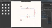
One of the most common points of failure of a device occurs even before you start to layout your circuit board. Mistakes in your schematic design can easily make their way all the way into prototypes or production without a second thought once layout starts. In this article, I’m not going to extol the virtues of a good schematic design. Instead, this article is a simple no frills checklist.

Read More
Via current carrying capacity for PCBs
Blog • Nov 11, 2021
PCB Via Current-Carrying Capacity: How Hot is Too Hot?

One common question from designers is current-carrying capacity of conductors in a PCB. Trace and via current-carrying capacity are legitimate design points to focus on when designing a new board that will carry high current. The goal is to keep conductor temperatures below some appropriate limit, which then helps keep components on the board cool. Let’s dig into the current state of thermal demands on vias in PCBs and how they compare to internal and external PCB traces.

Read More
PCB Shield
Blog • Nov 9, 2021
Phalanx, not Failure: PCB Shielding to Protect Your Design

A combination of good printed circuit board design and good shielding mitigates EMI. Good PCB design for EMI shielding revolves around the layout, the placement of filters, and ground planes. A well-designed PCB minimizes parasitic capacitance and ground loops. Keep reading to learn more about PCB shielding.

Read More
Man working in Altium Designer
Blog • Nov 4, 2021
Best Practices in Hardware Version Control Systems

Any project can get very complex, and the PCB design team needs to track revisions throughout a project. Why worry about tracking revisions? In the event you ever receive changes to product functional requirements, major changes are made to your product’s architecture, or you’re ready to finalize the design and prepare for fabrication, it’s best to clone a project at its current state and begin working on a new version. Keeping track of all these design changes in a PCB design project takes the type of hardware version control tools you’ll find in Altium 365™.

Read More
Copper pour and via stitching
Blog • Oct 28, 2021
Copper Pour and Via Stitching: Do You Need Them in a PCB Layout?

To pour or not to pour, to stitch or not to stitch… Over many years, some common “rules of thumb” have become very popular and, ultimately, taken a bit out of context. Rules of thumb are not always wrong, but taking PCB design recommendations out of context helps justify bad design practices, and it can even affect the producibility of your board. Like many aspects of a physical PCB layout, via stitching and copper pour can be like acid: quite useful if implemented properly, but also dangerous if used indiscriminately.

Read More
  • Show More
Tag (field_common_tag)
Embedded thumbnail for Using Polygons on Power Planes
New in Altium Designer 21 • Dec 28, 2020
Using Polygons on Power Planes

Traditionally, a PCB power plane is designed as a negative, that is, the objects placed on a power plane layer become voids in the copper when the board is fabricated. This approach is used because it is more efficient to generate the output data this way, as the bulk of a plane layer is normally copper; voids in the copper are only needed in specific locations such as around non-connected pads, or as separation voids when the plane is divided into different voltage regions.

Start Watching
Embedded thumbnail for Enhanced Polar Grid Support
New in Altium Designer 21 • Dec 28, 2020
Enhanced Polar Grid Support

Component placement is one of the main steps in board design. And in specific boards of a circular shape, it is convenient to use a polar grid for the location of components. Altium Designer 21 brings several improvements to the polar grid. Now, when a component is positioned in a polar grid, its properties additionally display location coordinates relative to this grid. Using them, you can quickly arrange the components in the right places. And moving the component off the grid, polar coordinates are automatically disabled.

Start Watching
Embedded thumbnail for New PCB Length Tuning Patterns
New in Altium Designer 21 • Dec 28, 2020
New PCB Length Tuning Patterns

Length matching is a critical element of high-speed design, usually solved by carefully tuning the lengths of critical routes. This release sees extensive improvements to both single-sided and differential pair length tuning capabilities. Length tuning now supports all three popular tuning patterns: Trombone, Sawtooth, and Accordion. If you are working with lower speed or lower frequency signals, you can get away with trombone tuning. For the Trombone patterns, the polygonal area that the pattern is constructed within can be thought of as a sleeve.

Start Watching
Embedded thumbnail for Expressions Library for Frequently Used Rules
New in Altium Designer 21 • Dec 28, 2020
Expressions Library for Frequently Used Rules

When working with design rules, we often use different scopes of the rules. To simplify the repetitive process of creating advanced type rules, the new Altium Designer 21 Rule Editor has the ability to save query-based object mapping scopes in a scoped library. To do this, it is enough to export the request by clicking on it with RMB. The library is presented through the Properties panel, where custom scopes can be edited, new ones added, and later reused in other custom constraint rules.

Start Watching
Embedded thumbnail for Constraint Rule Violations
New in Altium Designer 21 • Dec 28, 2020
Constraint Rule Violations

Enabled design constraint rules are applied to the current board design through a range of mechanisms, such as live Online Design Rule Checking, the batch Design Rule Checker or selectively run from the PCB Rules and Violations panel. Violations of those constraint Rules – where the specified and scoped limits are exceeded – are indicated through board graphics, panel entries and reports. With the introduction of a new Rules Editor in Altium Designer 21, violations of these rules are now displayed in the Rules Editor itself.

Start Watching
Embedded thumbnail for Table-based Approach for Design Rules and Constraints
New in Altium Designer 21 • Dec 28, 2020
Table-based Approach for Design Rules and Constraints

Define and assign a specific list of rules and constraints to all critical design elements, such as components, nets, and LVDS.

Start Watching
Embedded thumbnail for Comprehensive Simulation Model Support
New in Altium Designer 21 • Dec 28, 2020
Comprehensive Simulation Model Support

Having accurate SPICE models is critical to the success of your simulation. Altium Designer now supports analog PSpice, LTspice, and more including generic component SPICE models for when you can’t find company models. Generic components contain Spice model parameters to simplify simulation. When you are done with simulation, quickly replace your generic components with an existing component to finish your design.

Start Watching
Embedded thumbnail for Easy to Start Simulations
New in Altium Designer 21 • Dec 28, 2020
Easy to Start Simulations

0:00 Simulation Dashboard Panel Following on from the recent introduction of an advanced new SPICE Simulation engine for Altium Designer, the latest round of Simulation updates focuses on user interface. A major component of the Altium Designer Simulation user interface updates is the introduction of the Simulation Dashboard panel. The panel offers a greatly simplified approach to checking, configuring, running and reviewing simulations.

Start Watching
Embedded thumbnail for Rigid-Flex Board Planning Mode
New in Altium Designer 21 • Dec 28, 2020
Rigid-Flex Board Planning Mode

This new release of Altium Designer 21 includes significant improvements to the Rigid-Flex board designs. Along with many bug fixes and enhancements, the next phase of Altium Rigid-Flex technology development is providing functional improvements. It is now possible to create new board regions by primitives using the appropriate command from the Design » Board Shape menu. The properties of all created regions are now displayed in the Properties panel where you can edit the name of each region and define the previously created stacks for each region of the board.

Start Watching
Embedded thumbnail for Component Pin to Multiple Pad Mapping
New in Altium Designer 21 • Dec 28, 2020
Component Pin to Multiple Pad Mapping

This release introduces flexible pin to pad mapping capabilities for managed components. Enhancements to the Single Component Editor and the introduction of a new Pins panel allow component symbol pins to be mapped to any component footprint pad, or any number of footprint pads. The Pins panel, opened from the editor's button, allows the default one-to-one pin-pad mapping to be changed to a custom relationship, such as one pin being connected to multiple footprint pads – or any other non-aligned pin to pad number relationship.

Start Watching
Embedded thumbnail for Enhanced Navigation by Nets in Schematic - Altium Designer 21 What's New
New in Altium Designer 21 • Dec 28, 2020
Enhanced Navigation by Nets in Schematic - Altium Designer 21 What's New

Altium Designer 21 brings many improvements to the schematic editor aimed at visualizing circuits and improving navigation through them in multi-sheet and hierarchical designs. By holding Alt and clicking on the net, All schematic instances of the net are highlighted, while other objects are dimmed, to visibly indicate the signal/power propagation in the design using one simple action. The changes also affected the Identification of net names. Now logical and physical names of a net are displayed in the properties panel as well as when you hover over this wire.

Start Watching
Embedded thumbnail for Intelligent Schematic Insights
New in Altium Designer 21 • Dec 28, 2020
Intelligent Schematic Insights

Due to advances in the format and compilation of the Altium Designer data model, schematic Wire objects have now evolved from a simple graphical object to a more advanced form that can be directly associated with electrical parameters. As a result, the Wire mode of the Properties panel has been updated to provide an expanded set of options and a wider range of information. The new additions include a General section for net parameter options and information, and a Parameters section that lists the User Parameters, Rules and Net Classes associated with the Wire's assigned net.

Start Watching
Embedded thumbnail for Start Your Schematic with Generic Components
New in Altium Designer 21 • Dec 28, 2020
Start Your Schematic with Generic Components

It can be challenging to pick the right components when working on a new schematic. You have to consider availability, cost, and various parametric requirements. What if you could place a component to complete your design and quickly replace it when you are ready for layout? Introducing new Generic Components. Simply provide generic parameters, such as Value or Footprint, to greatly speed-up your capturing process while eliminating the need to search for specific Part Numbers or creating a needed component from scratch.

Start Watching
Embedded thumbnail for MCAD CoDesigner Overview
Working with MCAD CoDesigner extension • Dec 21, 2020
MCAD CoDesigner Overview

The MCAD CoDesigner in Altium Designer allows for seamless design transfer between the Electrical and Mechanical designers. In this overview, we’ll show you how to transfer from Altium Designer to your CAD tool of choice, then how to resize the board, add mounting holes, add a new connector, and update the board design in Altium Designer.

Start Watching
Embedded thumbnail for Bringing an MCAD Enclosure to ECAD
Working with MCAD CoDesigner extension • Nov 16, 2020
Bringing an MCAD Enclosure to ECAD

The Altium Designer MCAD CoDesigner panel and extension make it easy to move a 3D enclosure model from your MCAD tool to Altium Designer. We'll show you how and what to watch out for while your transferring your enclosure model to Altium Designer.

Start Watching
Embedded thumbnail for How to Perform a Component Search in Concord Pro - Altium Academy
How-To's • Oct 28, 2020
How to Perform a Component Search in Concord Pro - Altium Academy

In this video, I'll show you how to perform a component search in the Components Panel. Learn how to perform a component search in the Components Panel while using Altium Concord Pro to effectively host all your component libraries from Altium Designer. You can always locate any particular component using this library navigation and place it on your schematic with pricing information from global suppliers. This availability and pricing information gets updated daily directly from the suppliers so you will always get fresh, up to date information. 

Start Watching
  • Show More
Tag (field_common_tag)
 Preventing Obsolescence Before It Hits
On-Demand Webinar • Jun 12, 2025
Proactive Lifecycle Management: Preventing Obsolescence Before It Hits
Take the first step toward eliminating avoidable delays and costly redesigns. Don't miss it and register now!
Watch Now
Integrating Requirements June 2025 Webinar
On-Demand Webinar • May 28, 2025
Integrating Requirements into Your PCB Design Workflow
Join our webinar where you will learn about integrated requirements tools who can help you eliminate late-stage design changes, AI support through system requirements and integration of design requirements directly in PCB Design. Don't miss it, register now!
Watch Now
A365 Webinar
On-Demand Webinar • Apr 23, 2025
Collaborative Design Review: Ensuring Quality from Schematics to Supply Chain
Join our live webinar to learn how Altium 365 accelerates collaboration, standardizes workflows, and ensures design integrity to mitigate risks and accelerate time to market.
Watch Now
Webinar: From Prototype to Production: Optimizing BOM Costs Without Compromising Quality with Part Analytics
On-Demand Webinar • Apr 22, 2025
From Prototype to Production: Optimizing BOM Costs Without Compromising Quality with Part Analytics
Learn how to reduce production BOM costs without redesign, explore techniques to consolidate part demand for volume savings, and discover case examples from supply chain teams that increased sourcing process efficiency by up to 97%.
Watch Now
Streamlining Team Collaboration
On-Demand Webinar • Apr 17, 2025
Streamlining Team Collaboration in Industrial PCB Projects
Join us for our upcoming webinar to discover how Altium Designer and Altium 365 can transform your team’s collaboration and take your PCB design projects to the next level. Attend for a chance to win free access to the Altium 365 Training Bundle.
Watch Now
Component management
On-Demand Webinar • Apr 10, 2025
Ensure Best Designs with Professional Library Management
In this webinar, you'll discover how Altium Designer facilitates robust component management, including adding part choices to mitigate supply chain risks and leveraging Altium 365 managed components.
Watch Now
April 2025 Webinar Cover
On-Demand Webinar • Apr 9, 2025
Component Selection in Altium Designer: Making Data-Driven Decisions with Data Integrations
Improve component selection with real-time data insights in Altium 365! Join our live webinar to optimize your PCB development. Sign up now!
Watch Now
Live Webinar
TEST
Jan
30
English
2:41 AM, PST
Jan
31
English
12:00 PM, CET
Jan
31
German
3:00 PM, CET
Register Now
Altium Agile
Live Webinar
Altium Agile Teams - Sneak Peek
Get a first glimpse into this new Electronic Product Development Platform.
Jan
21
English
3:00 PM, CET
Jan
21
German
10:00 AM, CET
Jan
22
Italian
10:00 AM, CET
Jan
22
French
3:00 PM, CET
Jan
22
Spanish
3:00 PM, CET
Register Now
Altium Platform
On-Demand Webinar • Nov 21, 2025
Altium Platform - A foundation to meet your & your company’s targets
Discover how the Altium platform makes multidisciplinary cooperation easy and efficient.
Watch Now
Harness design
On-Demand Webinar • Nov 17, 2025
From single PCB to Harnessed Product
Discover how to streamline PCB-to-harness design with Altium’s powerful tools and boost collaboration across disciplines.
Watch Now
3D-MID Design
On-Demand Webinar • Oct 20, 2025
3D-MID Design in Altium
Discover how even complex products for 3D circuit designs are implemented easily in Altium.
Watch Now
Altium Designer Overview
On-Demand Webinar • Aug 20, 2025
Altium Designer and Altium 365 Overview
In this webinar we will show you how easy it is to create a prototype from scratch using Altium Designer in combination with Altium 365.
Watch Now
Altium Enterprise
On-Demand Webinar • Aug 3, 2025
Safety & Reliability in Electronics Design – Strategies, Standards & Tools
How can development teams and decision-makers effectively implement safety, security, and compliance without delaying innovation?
Watch Now
Altium Enterprise
On-Demand Webinar • Aug 2, 2025
Sustainability & Energy Efficiency in Electronic Product Development
Watch Now
Proactive Component Selection
On-Demand Webinar • May 22, 2025
Proactive Component Selection: Mitigating Manufacturing Delays Before They Happen
Most teams spend hours on component research yet still face redesigns. Learn how Altium 365 helps you make proactive, data-driven part decisions. Join SiliconExpert’s Jackie Sartin to discover smarter sourcing with real-time insights and validated alternatives.
Watch Now
  • Show More
Tag (field_common_tag)
Loading
Loading...
Share link
Share with
Search by Update
Version
Update
25 26 24 23 22
25.0 25.1 25.2 25.3 25.4 25.5 25.6 25.7 25.8 25.9
26.1 26.2
24.10 24.9 24.8 24.7 24.6 24.5 24.4 24.3 24.2 24.1 24.0
23.11 23.10 23.9 23.8 23.7 23.6 23.5 23.4 23.3 23.2 23.1 23.0
22.11 22.10 22.9 22.8 22.7 22.6 22.5 22.4 22.3