
Main navigation

  • Home
  • Discover
  • Learning Center
  • What’s New

Second main navigation

  • Altium Community
  • Support
  • Documentation
×

Results

  • Updates
  • Blog 570
  • Video 540
  • Webinar 87
  • Playlist 53
Filters:
Tag (field_common_tag)
Blog • Nov 4, 2025
6 Areas Your PCB Design Reviews Should Focus On

Learn the six essential topics every electronics team should address in design reviews to improve quality, avoid surprises and bring products to market faster.

Read More
Embedded thumbnail for Altium Training - Navigating Schematics: Schematic Preference Settings for Navigation
Altium Training • Nov 3, 2025
Altium Training - Navigating Schematics: Schematic Preference Settings for Navigation

Unlock smarter design navigation in Altium! Learn how to customize navigation preferences to boost your design insight and visualize connectivity like never before. In this video, we’ll explore Design Insight settings, interactive connectivity hover features, and quick thumbnail navigation between schematic sheets. All designed to make your workflow faster, clearer, and more intuitive.

Start Watching
Blog • Oct 30, 2025
What Is BOM Management? A Practical Guide to Avoiding Costly Part Mismatches

From design to production, effective Bill of Materials (BOM) management is critical to ensuring smooth collaboration between engineering, procurement, and manufacturing teams. In this practical guide, we break down proven strategies for structuring, maintaining, and synchronizing your BOM to prevent costly mistakes and accelerate time-to-market.

Read More
Blog • Oct 29, 2025
Requirements Portal Introductory Tutorials

This series of guided demos shows how the Altium Requirements Portal transforms scattered requirement spreadsheets and emails into traceable, version-controlled data that stays aligned with your PCB design efforts.

Read More
Embedded thumbnail for PCB Design Tools for Every Team Size: Altium's New Approach
How-To's • Oct 28, 2025
PCB Design Tools for Every Team Size: Altium's New Approach

Explore how Altium is transforming PCB design with software solutions built for teams of every size. In this exclusive PCB West 2025 interview, Justin Sears highlights the key distinctions between Altium Develop and Altium Agile helping you identify the ideal platform for your design needs.

Start Watching
Blog • Oct 27, 2025
Bridging the Gap: When to Use Rigid-Flex Instead of Flex & Connector

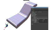
Discover when a rigid-flex PCB is a better choice than a separate flex circuit and connector, especially for designs requiring compact packaging, repeated motion or high reliability. The article emphasizes that although rigid-flex needs more upfront planning and fabrication collaboration, it often pays off in simpler assemblies and improved performance.

Read More
Embedded thumbnail for PCB Design: Sequential Lamination vs Sub-Lamination
How-To's • Oct 23, 2025
PCB Design: Sequential Lamination vs Sub-Lamination

Explore the key distinctions between sequential lamination and sub-lamination techniques, and learn how each approach influences microvia placement, board complexity, and design flexibility in high-density interconnect (HDI) circuit board fabrication.


Start Watching
Blog • Oct 22, 2025
Bridging Mechanical and Electrical Teams for Smarter Automotive Design

As vehicles evolve into advanced electronic systems, the separation between electrical and mechanical design teams becomes a critical bottleneck. This article explores how synchronized ECAD–MCAD workflows help automotive projects move faster, reduce rework and maintain design integrity.

Read More
Embedded thumbnail for PCB Design Review: Power Meter Layout Deep Dive
How-To's • Oct 21, 2025
PCB Design Review: Power Meter Layout Deep Dive

Gain practical insights into PCB design with an in-depth power meter project review, covering parameter optimization, BOM control, and IPC-compliant high-voltage spacing.

Start Watching
Blog • Oct 20, 2025
Via Structures: Designing for Reliability, Not Just Density

We all want to pack more into our PCB designs, but the smallest via isn’t always the smartest one. Dive in to learn how picking the right structure can save you headaches down the line.

Read More
Embedded thumbnail for Drawing Tools for Pro Schematics in Altium
How-To's • Oct 16, 2025
Drawing Tools for Pro Schematics in Altium

In our brand-new tutorial, you’ll learn how to create professional-looking schematics in Altium using built-in drawing tools and features. We’ll show you how to add custom title blocks, revision histories, tables of contents, block diagrams, and color schemes to make your schematics stand out.

Start Watching
Blog • Oct 15, 2025
How Structural Electronics Enables 3D, Flexible, and Wearable Integration

Structural electronics integrates electronic functionality directly into the physical structure of a product, eliminating the need for traditional circuit boards. This article examines how advances in materials, additive manufacturing, and flexible substrates are enabling compact, 3D, and wearable systems with enhanced performance and design freedom.

Read More
Embedded thumbnail for 3 GHz RF Amplifier Deep Dive
How-To's • Oct 14, 2025
3 GHz RF Amplifier Deep Dive

Check out our design review of a 3.6 GHz RF amplifier! This in-depth analysis highlights schematic issues, PCB layout challenges, and key RF design principles to help you build better high-frequency circuits.

Start Watching
Blog • Oct 9, 2025
Beyond Traces: Why Soldermask May Be the Critical Factor in Ultra HDI

In ultra-HDI designs, soldermask is no longer a passive coating but a pivotal element that can determine manufacturability. This article explores why mask registration, resolution, and feature tolerances become critical as line spacings shrink below 50 µm.

Read More
Embedded thumbnail for The Right Way to Use SIG/GND/PWR/SIG Stackups
How-To's • Oct 8, 2025
The Right Way to Use SIG/GND/PWR/SIG Stackups

Find out how to properly implement signal-ground-power-signal stackups in 4-layer PCB designs. Check out our tutorial from Zach Peterson, where he explains when to use dedicated power layers, how to route signals correctly over split power planes, and common mistakes to avoid for optimal EMI performance and signal integrity.

Start Watching
Blog • Oct 7, 2025
How ECAD-MCAD Co-Design Supports Aerospace Reliability and Compliance

When the margin for error is nearly zero, aerospace engineering demands a design process that’s seamless across all domains. Here, we explore how ECAD-MCAD co-design delivers an integrated workflow that supports first-pass success and compliance with strict aerospace standards.

Read More
  • Show More
Tag (field_common_tag)
Altium 365 SOC 2 Type 1 Certified
Blog • Feb 15, 2022
Announcing SOC 2 Type 1 Certification for Altium 365

We are pleased to announce that Altium 365 is officially SOC 2 Type 1 certified. System and Organization Controls (SOC) 2 is a widely recognized attestation of security compliance defined by the AICPA and is considered the standard for ensuring data security and operational maturity. A SOC 2 certification provides valuable information for companies to assess the quality of the security provided by a service such as Altium 365.

Read More
Three ways to manage your BOM costs
Blog • Feb 10, 2022
Improving Supply Chain Success with BOM Management

It’s no secret that component shortages have become more frequent this year. Companies will continue to grapple with supply chain challenges into 2022 and beyond. The impact of manufacturing delays can be substantial if a part is not available. Delays occur and sales plans get put on hold. It can also be very expensive and risky to replace parts from multiple sources. Fortunately, many shortages can be avoided by introducing proactive supply chain practices.

Read More
Reliability and failure analysis
Blog • Feb 8, 2022
Overview of PCB/PCBA Reliability and Failure Analysis

Reliability testing and failure analysis of a PCB/PCBA go hand-in-hand; when designs are stressed to the limit, their failure modes need to be determined through thorough inspection and analysis. To get started on this topic, it’s important to understand the qualification aspects that will govern your bare board design and the PCBA. We’ll look at the various dimensions of PCB/PCBA reliability, as well as some of the standard failure analysis techniques used to identify potential design change requirements.

Read More
Plane and Cavity Resonances
Blog • Feb 3, 2022
When Do PCB Power Plane Resonances Occur?

By now, designers should be aware of some important behavior involved in power delivery to components in a PCB, particularly for digital components. All digital components produce and manipulate wideband signals, where the frequency content theoretically extends up to infinite frequency. As such, some radiation may propagate through your PCB, leading to resonant behavior that is not observed on the power rail.

Read More
Selecting a plating material
Blog • Feb 1, 2022
How to Choose PCB Plating for Your Finished Board

Once your board passes through the standard PCB fabrication process, the bare copper in your PCB will be ready for the application of a surface finish. PCB plating is applied to protect any copper in your PCB that would be exposed through the solder mask, whether it’s a pad, via, or other conductive element. In this article, I’ll run over the different PCB plating material options and their advantages in your PCB. 

Read More
What is the PCB Supply Chain?
Blog • Jan 27, 2022
What is the PCB Supply Chain?

The PCB supply chain encompasses multiple components, raw materials, and the PCB itself. PCBs and PCB assemblies are often the most technically complex components that are purchased for electronic assemblies and products. The complexity of modern PCBs leads to several challenges for a supply chain management team that may be significantly different when compared with other commodities the team manages. In this brief guide, we'll look in-depth at the PCB supply chain, and specifically what falls within the purview of a procurement and supply chain management team.

Read More
What is mode conversion
Blog • Jan 25, 2022
A Guide to Mode Conversion, Its Causes, and Solutions

On interconnects, such as board-to-board connections or cascaded transmission line arrangements, you have an important EMC compliance metric that is sometimes overlooked. This is mode conversion, which can be visualized in an S-parameter measurement for differential and common-mode signal transmission. In this article, we’ll look at a short overview of mode conversion in high-speed design with some examples from common differential standards.

Read More
Pad and via sizing
Blog • Jan 20, 2022
PCB Via Size and Pad Size Guidelines

There are some aspects of PCB design and layout that seem deceptively simple, and yet they have a complex answer that is related to many important aspects of manufacturing. One of these design aspects is the match between PCB via size and pad size. Obviously, these two points are related; all vias have a landing pad that supports the via and provides a place to route traces into a via pad. However, there are some important sizing guidelines to follow when the matching pad and via sizes, and this match is an important element of DFM and reliability.

Read More
Differential Microstrip Impedance
Blog • Jan 18, 2022
Differential Microstrip Impedance Calculator

Are you looking for a free tool that you can use to calculate the impedance of differential microstrips? We created a simple tool you can use to calculate differential microstrip impedance for a given geometry and dielectric constant. If you’ve been looking for an accurate differential microstrip impedance calculator, then the calculator below is certainly one of the best free tools you’ll find on the internet before you start using field solvers to determine differential pair impedance.

Read More
PCB DFM Check
Blog • Jan 13, 2022
Getting Through a PCB DFM Check

In this article, we’ll discuss the key design features to implement, and steps to take prior to fabrication that will help prevent some common DFM problems. I’ll also provide examples of where I commonly see these PCB DFM problems in signal integrity circuits.

Read More
Spreading Inductance
Blog • Jan 11, 2022
What is Spreading Inductance?

If you’re working with a high-speed digital component, there are some simple power integrity rules that should be followed. However, there is one quantity that is sometimes ignored when building a PDN impedance simulation: the spreading inductance of your plane pair. Here are some points designers should know about the spreading inductance of a plane pair.

Read More
PCB Design Basics for New Designers
Blog • Jan 6, 2022
PCB Design Basics for New Designers

In this article, I’ll present some design basics that every new designer should follow to help ensure their design process is successful. Some of these points may challenge the conventional view of how circuit boards are constructed, but they are intended to help balance low noise signaling, manufacturability, and ease of solving a layout.

Read More
Selecting Materials for High Voltage PCB Design and Layout
Blog • Jan 4, 2022
Selecting Materials for High Voltage PCB Design and Layout

High voltage PCBs are subject to certain safety and reliability concerns that you won’t find in most other boards. If your fabrication house specializes in high voltage PCBs and keeps materials in stock, they can likely recommend a material set, as well as a standard stackup you might use for certain voltage ranges and frequencies. If you need to choose your own materials, follow the tips below to help you narrow down to the right material set.

Read More
Via tenting in PCB Layout
Blog • Dec 28, 2021
When to Use Tented Vias in Your PCB Layout

There are some guidelines I see many designers implement as a standard practice, often without thinking about it. Some of these practices are misunderstood or implemented without best practices. Others are implemented without thinking about the potential problems. One of these is the use of tented vias, which is sometimes implemented in a PCB layout by default. Is this always the right practice?

Read More
Capacitive load termination
Blog • Dec 23, 2021
How to Impedance Match and Terminate Capacitive Loads

The idea of a purely capacitive load is something of a fallacy. Yes, capacitors exist, but all capacitors are non-ideal, and it is this deviation from a theoretical capacitance that determines how to impedance match a load that exhibits capacitive behavior. Let’s take a look at this important aspect of interconnect design and see what it really means to terminate a capacitive load.

Read More
Using Altium 365 Over Your Vanilla Version Control System
Blog • Dec 20, 2021
Using Altium 365 Over Your Vanilla Version Control System

There are all sorts of version control systems out there that people have been using with their PCB design software. As discussed in Why Use a Version Control System, we looked at different options ranging for local hard drive storage to sophisticated online revisioning systems. In this article we will be reviewing the differences between a standard VCS and Altium 365.

Read More
  • Show More
Tag (field_common_tag)
Embedded thumbnail for Snapping When Creating Polygons
How to use Snapping • Oct 23, 2020
Snapping When Creating Polygons

When creating polygons you can use snap points to form fit your polygons to the exact size and shape you need. We’ll show you how to set your snap points, which ones are most helpful for creating polygons, and how to use the same techniques to create keep out and solder mask areas.

Start Watching
Embedded thumbnail for Automatic Symbol Creation in Altium 365
Library Managment • Oct 19, 2020
Automatic Symbol Creation in Altium 365

In order to design your projects, you’ll need a set of components to work with. Although the integration of Octopart with Altium Designer gives us a large repertoire of components, you simply can’t have access to every component model in the world. We’re going to create a component in the Altium 365 workspace with the Symbol Creation Wizard.

Start Watching
Embedded thumbnail for Creating Differential Pairs in the PCB
How to Work with Differential Pairs • Aug 21, 2020
Creating Differential Pairs in the PCB

Learn how to create differential pairs in the PCB.

Start Watching
Embedded thumbnail for From The Beatles to the PCB - VOX Story
Success Stories • Aug 19, 2020
From The Beatles to the PCB - VOX Story

Dave Clarke, R&D manager for VOX, walks us through his story of designing VOX amplifiers for electronic instruments as well as his love for music and electronics design. Be sure to subscribe to the Altium Stories channel to stay updated on new videos. Altium LLC is accelerating the pace of innovation through electronics. From individual inventors to multinational corporations, more PCB designers and engineers choose Altium software to design and realize their ideas. 

Start Watching
Embedded thumbnail for Creating PCB Mounting Holes
• Jul 29, 2020
Creating PCB Mounting Holes

Our PCB must somehow be assembled into the final drone assembly. This will be achieved by attaching our PCB to the motherboard connector and by special mounting racks, which requires precise positioning of the two mounting holes on the PCB.

Start Watching
Embedded thumbnail for Working with PCB Keepouts
• Jul 24, 2020
Working with PCB Keepouts

When working in the PCB, there may be specific areas that you would want to prevent the presence of certain objects, such as vias, tracks or copper regions. All of this can be realized in Altium Designer by using the Keepouts feature.

Start Watching
Embedded thumbnail for Local PCB Library & Footprint Creation
Library Managment • Jul 22, 2020
Local PCB Library & Footprint Creation

We’ve already looked at how to create a footprint from scratch, but with the help of the IPC Footprint Wizard, you can create any IPC compliant component by entering a bit of information which is what we’ll be covering.

Start Watching
Embedded thumbnail for Manual Footprint Creation with Altium 365
Library Managment • Jul 22, 2020
Manual Footprint Creation with Altium 365

A footprint or land pattern represents the real-world copper or through-hole component pads that get mounted on the board. We’re going to cover nearly everything that’s needed to create a footprint from scratch and add it to our USB component that’ll be stored in our Altium 365 workspace.

Start Watching
Embedded thumbnail for Local Library and Symbol Creation
Library Managment • Jul 22, 2020
Local Library and Symbol Creation

In the last video, we created a component with a schematic symbol stored in the Altium 365 workspace. Now, we’re going to cover the process of creating a local schematic library with a schematic symbol for our Workspace.

Start Watching
Embedded thumbnail for Generating and Storing Outputs
• Jun 23, 2020
Generating and Storing Outputs

Once our manufacturing and assembly outputs have been configured, we’re ready to generate these outputs that will be stored in the project folder and ready to be sent out to manufacturing.

Start Watching
Embedded thumbnail for Preparing Assembly Outputs
• Jun 23, 2020
Preparing Assembly Outputs

Once you've looked at the fabrication outputs for your PCB, it is time to look at the files needed for the Assembly process. This includes Assembly Drawings, Pick & Place files, and more.

Start Watching
Embedded thumbnail for Preparing Fabrication Outputs
• Jun 23, 2020
Preparing Fabrication Outputs

The files generated in this section are going to be sent to the PCB manufacturer, where they’ll be used to create the bare board. There are a few different files that need to be generated such as Gerbers, NC Drill files, and more.

Start Watching
Embedded thumbnail for Preparing Documentation Outputs
• Jun 23, 2020
Preparing Documentation Outputs

Aside from manufacturing and assembly outputs, you’ll likely want to generate some design documentation as well. We’ll configure outputs for some schematic prints and a bill of materials.

Start Watching
Embedded thumbnail for Creating an Outjob File
• Jun 23, 2020
Creating an Outjob File

Learn how to create documentation for the PCB manufacturer and assembly house. These files can now be generated individually, but it’s much faster and easier to use the OutJob file to output all the files in a central location.

Start Watching
Embedded thumbnail for Design Review Use Case
Discovering Altium 365 • Jun 19, 2020
Design Review Use Case

Design reviews are critical to being successful. Capture design discussions through contextual commenting in the web browser or in Altium Designer to ensure feedback is recorded and actioned effectively.

Start Watching
Embedded thumbnail for Resolving Errors in the PCB
• Jun 17, 2020
Resolving Errors in the PCB

We’ve looked at how to set up the Design Rule Checker to help us analyze our PCB design errors. Now it’s time to resolve these errors and prep our design to start generating output files.

Start Watching
  • Show More
Tag (field_common_tag)
 Preventing Obsolescence Before It Hits
On-Demand Webinar • Jun 12, 2025
Proactive Lifecycle Management: Preventing Obsolescence Before It Hits
Take the first step toward eliminating avoidable delays and costly redesigns. Don't miss it and register now!
Watch Now
Integrating Requirements June 2025 Webinar
On-Demand Webinar • May 28, 2025
Integrating Requirements into Your PCB Design Workflow
Join our webinar where you will learn about integrated requirements tools who can help you eliminate late-stage design changes, AI support through system requirements and integration of design requirements directly in PCB Design. Don't miss it, register now!
Watch Now
A365 Webinar
On-Demand Webinar • Apr 23, 2025
Collaborative Design Review: Ensuring Quality from Schematics to Supply Chain
Join our live webinar to learn how Altium 365 accelerates collaboration, standardizes workflows, and ensures design integrity to mitigate risks and accelerate time to market.
Watch Now
Webinar: From Prototype to Production: Optimizing BOM Costs Without Compromising Quality with Part Analytics
On-Demand Webinar • Apr 22, 2025
From Prototype to Production: Optimizing BOM Costs Without Compromising Quality with Part Analytics
Learn how to reduce production BOM costs without redesign, explore techniques to consolidate part demand for volume savings, and discover case examples from supply chain teams that increased sourcing process efficiency by up to 97%.
Watch Now
Streamlining Team Collaboration
On-Demand Webinar • Apr 17, 2025
Streamlining Team Collaboration in Industrial PCB Projects
Join us for our upcoming webinar to discover how Altium Designer and Altium 365 can transform your team’s collaboration and take your PCB design projects to the next level. Attend for a chance to win free access to the Altium 365 Training Bundle.
Watch Now
Component management
On-Demand Webinar • Apr 10, 2025
Ensure Best Designs with Professional Library Management
In this webinar, you'll discover how Altium Designer facilitates robust component management, including adding part choices to mitigate supply chain risks and leveraging Altium 365 managed components.
Watch Now
April 2025 Webinar Cover
On-Demand Webinar • Apr 9, 2025
Component Selection in Altium Designer: Making Data-Driven Decisions with Data Integrations
Improve component selection with real-time data insights in Altium 365! Join our live webinar to optimize your PCB development. Sign up now!
Watch Now
Live Webinar
TEST
Jan
30
English
2:41 AM, PST
Jan
31
English
12:00 PM, CET
Jan
31
German
3:00 PM, CET
Register Now
Altium Agile
Live Webinar
Altium Agile Teams - Sneak Peek
Get a first glimpse into this new Electronic Product Development Platform.
Jan
21
English
3:00 PM, CET
Jan
21
German
10:00 AM, CET
Jan
22
Italian
10:00 AM, CET
Jan
22
French
3:00 PM, CET
Jan
22
Spanish
3:00 PM, CET
Register Now
Altium Designer Overview
On-Demand Webinar • Dec 4, 2025
Altium Designer Onboarding Workshop
Join our live training workshop and see Altium Designer in action—from creating your first schematic to delivering ready-to-manufacture PCB files.
Watch Now
Altium Platform
On-Demand Webinar • Nov 21, 2025
Altium Platform - A foundation to meet your & your company’s targets
Discover how the Altium platform makes multidisciplinary cooperation easy and efficient.
Watch Now
Harness design
On-Demand Webinar • Nov 17, 2025
From single PCB to Harnessed Product
Discover how to streamline PCB-to-harness design with Altium’s powerful tools and boost collaboration across disciplines.
Watch Now
3D-MID Design
On-Demand Webinar • Oct 20, 2025
3D-MID Design in Altium
Discover how even complex products for 3D circuit designs are implemented easily in Altium.
Watch Now
Altium Designer Overview
On-Demand Webinar • Aug 20, 2025
Altium Designer and Altium 365 Overview
In this webinar we will show you how easy it is to create a prototype from scratch using Altium Designer in combination with Altium 365.
Watch Now
Altium Enterprise
On-Demand Webinar • Aug 3, 2025
Safety & Reliability in Electronics Design – Strategies, Standards & Tools
How can development teams and decision-makers effectively implement safety, security, and compliance without delaying innovation?
Watch Now
Altium Enterprise
On-Demand Webinar • Aug 2, 2025
Sustainability & Energy Efficiency in Electronic Product Development
Watch Now
  • Show More
Tag (field_common_tag)
Loading
Loading...
Share link
Share with
Search by Update
Version
Update
25 26 24 23 22
25.0 25.1 25.2 25.3 25.4 25.5 25.6 25.7 25.8 25.9
26.1 26.2
24.10 24.9 24.8 24.7 24.6 24.5 24.4 24.3 24.2 24.1 24.0
23.11 23.10 23.9 23.8 23.7 23.6 23.5 23.4 23.3 23.2 23.1 23.0
22.11 22.10 22.9 22.8 22.7 22.6 22.5 22.4 22.3